Metallization method of N-type solar cell, cell, module and system
A solar cell and metallization technology, which is applied in the field of solar cells, can solve the problems of high silver content and reduce the use of silver-containing paste, and achieve the effects of meeting soldering requirements, reducing front silver consumption, and excellent ohmic contact
- Summary
- Abstract
- Description
- Claims
- Application Information
AI Technical Summary
Problems solved by technology
Method used
Image

Examples
Embodiment 1
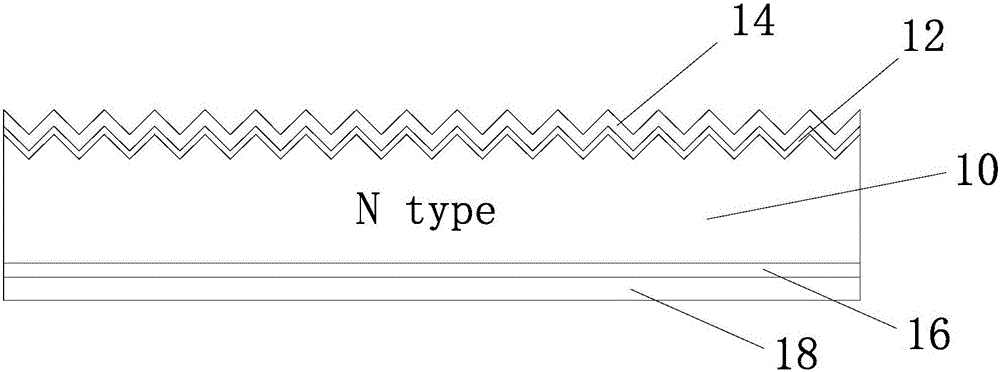
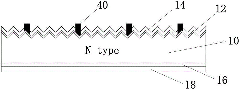
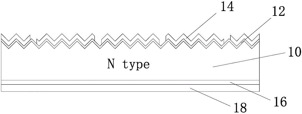
[0033] see figure 1 , Figure 3 to Figure 6 As shown, a metallization method of an N-type solar cell in this embodiment includes the following steps:
[0034] (1), such as figure 1 As shown, the N-type double-sided battery before metallization is prepared, including an N-type crystalline silicon substrate 10, and the front surface of the N-type crystalline silicon substrate 10 includes a p+ doped region 12 and a passivation anti-reflection film on the front surface in sequence from inside to outside. 14; the back surface of the N-type crystalline silicon substrate includes an n+ doped region 16 and a passivation film 18 on the back surface sequentially from inside to outside. Wherein the passivation anti-reflection film 14 on the front surface is SiO 2 , SiNx or Al 2 o 3 One or more of the dielectric films, the passivation film 18 on the back surface is SiO 2 and SiN x Composite dielectric membrane composed of dielectric membrane. The thickness of the N-type crystallin...
Embodiment 2
[0041] see Figure 1 to Figure 6 As shown, a metallization method of an N-type solar cell in this embodiment includes the following steps:
[0042] (1), such as figure 1 As shown, the N-type double-sided battery before metallization is prepared, including an N-type crystalline silicon substrate 10, and the front surface of the N-type crystalline silicon substrate 10 includes a p+ doped region 12 and a passivation anti-reflection film on the front surface in sequence from inside to outside. 14; the back surface of the N-type crystalline silicon substrate includes an n+ doped region 16 and a passivation film 18 on the back surface sequentially from inside to outside. Wherein the passivation anti-reflection film 14 on the front surface is SiO 2 , SiNx or Al 2 o 3 One or more of the dielectric films, the passivation film 18 on the back surface is SiO 2 and SiN x Composite dielectric membrane composed of dielectric membrane. The thickness of the N-type crystalline silicon su...
PUM
| Property | Measurement | Unit |
|---|---|---|
| Width | aaaaa | aaaaa |
| Thickness | aaaaa | aaaaa |
| Thickness | aaaaa | aaaaa |
Abstract
Description
Claims
Application Information