Transverse SOI power LDMOS

A lateral and power technology, applied in electrical components, circuits, semiconductor devices, etc., can solve the problems of charge imbalance sensitivity, substrate auxiliary depletion, device breakdown voltage drop, etc., to reduce on-resistance, reduce channel Channel resistance, drift region resistance, and on-resistance reduction effect

Inactive Publication Date: 2016-07-20
UNIV OF ELECTRONIC SCI & TECH OF CHINA
View PDF6 Cites 9 Cited by
  • Summary
  • Abstract
  • Description
  • Claims
  • Application Information

AI Technical Summary

Problems solved by technology

However, the superjunction has the following two disadvantages: 1. The breakdown voltage of the superjunction device is sensitive to charge imbalance, and the concentration deviation in the actual process will cause the breakdown voltage of the device to drop sharply; 2. For the lateral superjunction device substrate assisted depletion
[0008] The RESURF, super junction and field pl

Method used


Image

  • Transverse SOI power LDMOS
  • Transverse SOI power LDMOS
  • Transverse SOI power LDMOS

Examples


Embodiment 1

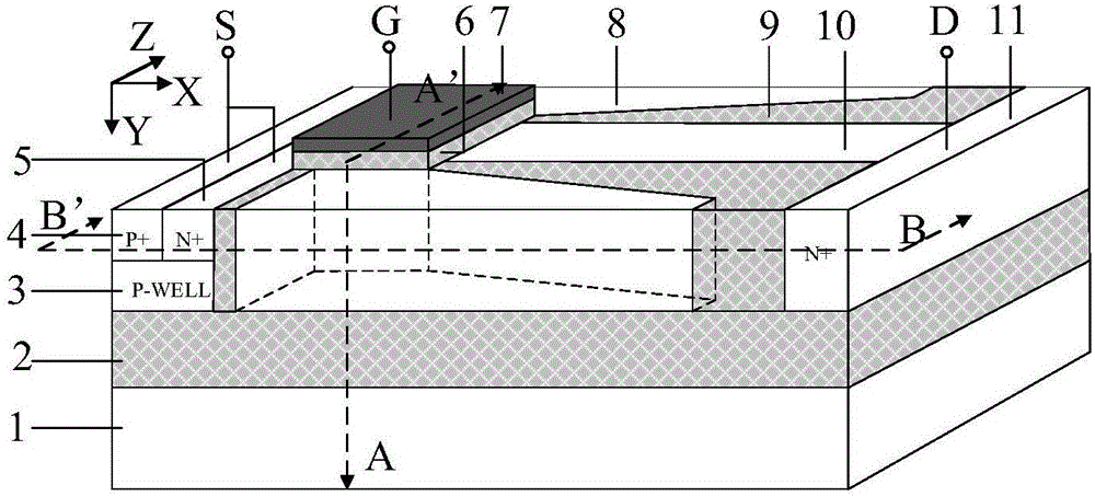
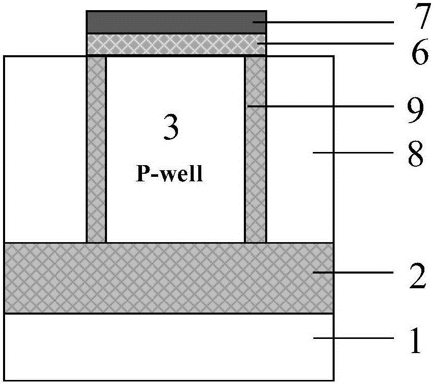
[0031] Such as figure 1As shown, the structure of this example includes a substrate layer 1 and a dielectric buried layer 2 positioned on the upper surface of the substrate layer 1; one end of the upper surface of the dielectric buried layer 2 has a P-type semiconductor body region 3, and the other end of the dielectric buried layer 2 upper surface One end has an N-type semiconductor drain region 11; the upper surface of the dielectric buried layer 2 between the P-type semiconductor body region 3 and the N-type semiconductor drain region 11 has a drift region 10; the upper surface of the P-type semiconductor body region 3 is far away from the drift region One side of 10 has a P-type semiconductor heavily doped contact region 4 and an N-type semiconductor heavily doped source region 5, the P-type semiconductor heavily doped contact region 4 and the N-type semiconductor heavily doped source region 5 are independent of each other and the N-type semiconductor The heavily doped sou...

Embodiment 2

[0035] Such as Figure 4 As shown, compared with Embodiment 1, the composite gate structure of this embodiment extends to the drift region in a stepped shape. It is beneficial to reduce the process difficulty of the composite groove structure.

Embodiment 3

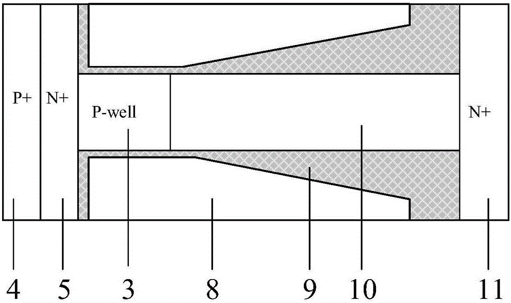
[0037] Such as Figure 5 As shown, compared with Embodiment 1, the drift region 10 of this example is not uniformly doped, and its doping concentration gradually increases from source to drain. The structure of variable doping in the drift region is beneficial to improve the withstand voltage of the device.


PUM


Abstract

The invention belongs to the technical field of semiconductor power devices, and relates to a transverse SOI power LDMOS. Compared with the existing structure, the power LDMOS provided by the invention has a three-dimensional gate structure, and an oxide layer thickness between the part extending to a trench gate field plate of a drift region from a gate and the drift region gradually changes from the gate to a drain end. In a forward conducting state, the trench gate forms a side channel to greatly reduce the channel resistance of the device; an electron accumulation layer is formed in the drift region to constitute a low resistance current channel, so as to greatly reduce the resistance in the drift region of the device; and the conducting resistance of the device is reduced by the two aspects. In a forward blocking state, the trench gate field plate extending to the drift region has a depletion effect on the drift region, thereby improving the concentration in the drift region and reducing the resistance in the drift region. Since most open state current flows by a charge accumulation layer, the specific on-state resistance of the transverse SOI power LDMOS provided by the invention is nearly not affected by the concentration in the drift region, so that the 2.5 power contradictory relationship of the specific on-state resistance Ron, sp of the device and the withstand voltage BV.

Description

technical field [0001] The invention belongs to the technical field of semiconductor power devices and relates to a lateral SOI power LDMOS. Background technique [0002] SOI refers to a semiconductor on an insulating substrate. Compared with bulk silicon technology, SOI technology has the advantages of high speed, low power consumption, high integration, small parasitic effects, small leakage current, and easy isolation, and has strong radiation resistance. Illumination ability and no SCR self-locking effect. At the same time, its relatively low on-resistance and ease of integration make SOILDMOS widely used in power integrated circuits, especially in low-power integrated circuits. [0003] For conventional LDMOS devices, the length of the drift region monotonically increases with the breakdown voltage of the device, thereby increasing the chip area and cost occupied by the device. More importantly, the on-resistance of the device increases with the increase of the drift ...

Claims


Application Information

Patent Timeline
IPC IPC(8): H01L29/78H01L29/06
CPCH01L29/7825H01L29/0692H01L29/7816
Inventor 罗小蓉吴俊峰马达魏杰
Owner UNIV OF ELECTRONIC SCI & TECH OF CHINA
Why Eureka
Try Eureka