Wide-spectrum quantum cascade infrared detector

An infrared detector and quantum cascade technology, which is applied in the field of infrared detectors, can solve the problems of device detection rate decrease, dark current increase, etc., and achieve the effect of quantum efficiency improvement, accurate output and reading

Inactive Publication Date: 2016-07-20
SHANGHAI INST OF TECHNICAL PHYSICS - CHINESE ACAD OF SCI
View PDF4 Cites 0 Cited by
  • Summary
  • Abstract
  • Description
  • Claims
  • Application Information

AI Technical Summary

Problems solved by technology

[0003] The basic principle of quantum well infrared detector determines that the quantum efficiency of the device is proportional to the absorption coefficient. In order to improve the quantum efficiency of the device, or to greatly increase the responsivity under similar detection conditions, it is necessary to increase the electrons on the ground state of the quantum well. concentration, but the increase of electron concentration directly increases the dark current superlinearly, which directly leads to the decrease of the detection rate of the device.

Method used


Image

  • Wide-spectrum quantum cascade infrared detector
  • Wide-spectrum quantum cascade infrared detector
  • Wide-spectrum quantum cascade infrared detector

Examples


example 1

[0030] (1) Growth of thin film materials for multiple quantum well chips:

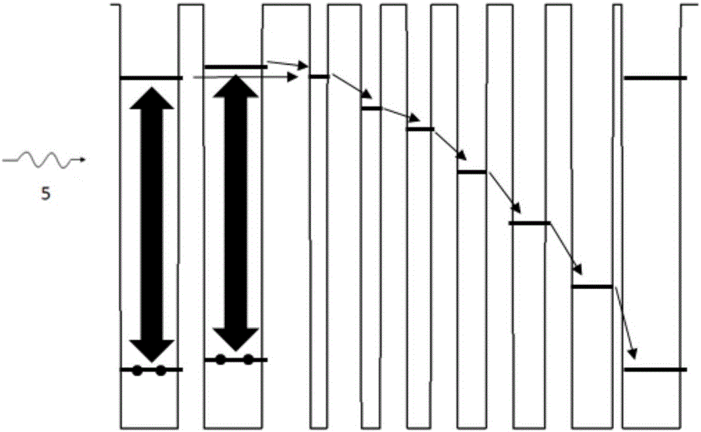
[0031] The following structure is sequentially grown on the GaAs substrate 1 by molecular number epitaxy (MBE), C 1 For GaAs:Si, the concentration is 10 18 / cm 3 , with a thickness of 0.5 μm; L 1 for Al 0.33 Ga 0.67 As, 40nm thick; QW 1 For GaAs:Si, the concentration is 10 17 / cm 3 , with a thickness of 6.8nm; L 1 ’ for Al 0.33 Ga 0.67 As, 3nm thick; QW 2 For GaAs:Si, the concentration is 10 17 / cm 3 , with a thickness of 6.8nm; L 2 ’ for Al 0.33 Ga 0.67 As, with a thickness of 5.65nm; QW 3 For GaAs, the thickness is 2nm; L 3 ’ for Al 0.33 Ga 0.67 As, with a thickness of 3.96nm; QW 4 For GaAs, the thickness is 2.3nm; L 4 ’ for Al 0.33 Ga 0.67 As, with a thickness of 3.1nm; QW 5 For GaAs, the thickness is 2.8nm; L 5 ’ for Al 0.33 Ga 0.67 As, with a thickness of 3.1nm; QW 6 For GaAs, the thickness is 3.4nm; L 6 ’ for Al 0.33 Ga 0.67 As, with a thickness of 3.1nm; QW 7For G...

example 2

[0038] (1) Growth of thin film materials for multiple quantum well chips:

[0039] The following structure is sequentially grown on the GaAs substrate 1 by molecular number epitaxy (MBE), C 1 For GaAs:Si, the concentration is 10 18 / cm 3 , with a thickness of 0.7 μm; L 1 for Al 0.32 Ga 0.68 As, 50nm thick; QW 1 For GaAs:Si, the concentration is 10 17 / cm 3 , with a thickness of 6.9nm; L 1 ’ for Al 0.32 Ga 0.68 As, 4nm thick; QW 2 For GaAs:Si, the concentration is 10 17 / cm 3 , with a thickness of 6.9nm; L 2 ’ for Al 0.32 Ga 0.68 As, with a thickness of 5.8nm; QW 3 For GaAs, the thickness is 2.2nm; L 3 ’ for Al 0.32 Ga 0.68 As, with a thickness of 4.1nm; QW 4 For GaAs, the thickness is 2.5nm; L 4 ’ for Al 0.32 Ga 0.68 As, with a thickness of 3.3nm; QW 5 For GaAs, the thickness is 3nm; L 5 ’ for Al 0.32 Ga 0.68 As, with a thickness of 3.3nm; QW 6 For GaAs, the thickness is 3.5nm; L 6 ’ for Al 0.32 Ga 0.68 As, with a thickness of 3.3nm; QW 7 For Ga...

example 3

[0046] (1) Growth of thin film materials for multiple quantum well chips:

[0047] The following structure is sequentially grown on the GaAs substrate 1 by molecular number epitaxy (MBE), C 1 For GaAs:Si, the concentration is 10 18 / cm 3 , with a thickness of 1 μm; L 1 for Al 0.31 Ga 0.69 As, 60nm thick; QW 1 For GaAs:Si, the concentration is 10 17 / cm 3 , with a thickness of 7nm; L 1 ’ for Al 0.31 Ga 0.69 As, with a thickness of 3.5nm; QW 2 For GaAs:Si, the concentration is 10 17 / cm 3 , with a thickness of 7nm; L 2 ’ for Al 0.31 Ga 0.69 As, 6nm thick; QW 3 For GaAs, the thickness is 2.4nm; L 3 ’ for Al 0.31 Ga 0.69 As, with a thickness of 4.3nm; QW 4 For GaAs, the thickness is 2.7nm; L 4 ’ for Al 0.31 Ga 0.69 As, with a thickness of 3.5nm; QW 5 For GaAs, the thickness is 3.2nm; L 5 ’ for Al 0.31 Ga 0.69 As, with a thickness of 3.5nm; QW 6 For GaAs, the thickness is 3.7nm; L 6 ’ for Al 0.31 Ga 0.69 As, with a thickness of 3.5nm; QW 7 For GaAs, ...


PUM


Abstract

The invention discloses a wide-spectrum quantum cascade infrared detector, which is composed of a compound semiconductor material substrate, barrier layers, quantum well layers and multiple quantum wells, wherein the eight barrier layers and quantum well layers with different widths are alternatively grown on the substrate to form a period, and multiple periods of quantum wells are grown repeatedly. Since the wide-spectrum quantum cascade infrared detector adopts a microstrip structure as an absorption region, a light response spectrum wider than that of an existing quantum cascade detector can be formed in the quantum well region at a low temperature under the irradiation of infrared light, and then the wide-spectrum quantum cascade infrared detector is more suitable for wide-spectrum detection application.

Description

technical field [0001] The invention relates to an infrared detector, in particular to a multi-quantum well infrared detector and a quantum cascade detector. Background technique [0002] In the current quantum infrared focal plane technology, the photosensitive element chip is composed of a number of photoconductive type spatially electrically and optically separated detector pixels. Compared with mercury cadmium telluride detectors, quantum well infrared detectors have the advantages of material growth and mature technology, good uniformity of large-area arrays, high yield, and low cost, but the quantum efficiency is low, so that the responsivity is low. Therefore, the optimization of quantum efficiency and responsivity is particularly important. [0003] The basic principle of quantum well infrared detector determines that the quantum efficiency of the device is proportional to the absorption coefficient. In order to improve the quantum efficiency of the device, or to gr...

Claims


Application Information

Patent Timeline
Patent Type & Authority Applications(China)
IPC IPC(8): H01L31/0352H01L31/101
CPCH01L31/035236H01L31/101
Inventor 周孝好李梁温洁郑元辽周玉伟李宁李志锋甄红楼陈平平陆卫
Owner SHANGHAI INST OF TECHNICAL PHYSICS - CHINESE ACAD OF SCI
Why Eureka
Try Eureka