

Aluminum-free type II superlattice long wave double-barrier infrared detector
A superlattice and double-barrier technology, applied in the field of infrared detectors, can solve the problems of low surface mobility and reduce the electrical performance of devices, and achieve the effect of low surface mobility, reduce dark current and improve electrical performance
- Summary
- Abstract
- Description
- Claims
- Application Information
AI Technical Summary
Problems solved by technology
Method used
Image

Examples
Embodiment 1
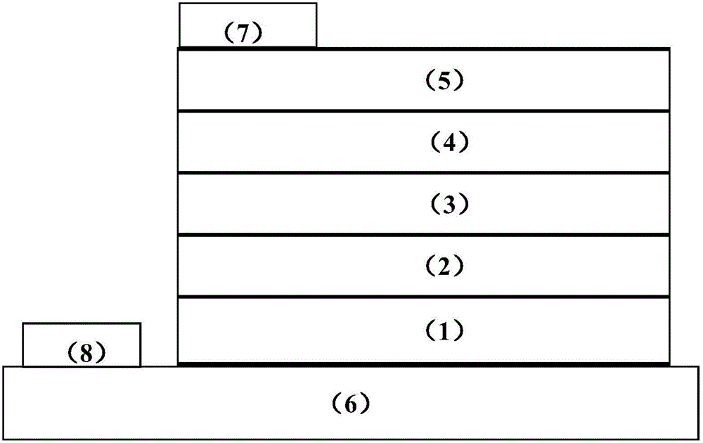
[0017] According to the content of the invention, we have prepared an aluminum-free long-wave double barrier superlattice infrared detector, the specific structure is as follows:
[0018] The superlattice long-wave N-type contact layer has 20 periods, each period is composed of 4nmInAs and 2nmGaSb, and the N-type doping concentration is 10 16 cm -3 ;
[0019] The superlattice hole barrier layer is 20 periods, each period is composed of 2nmInAs and 1nmGaSb, and the N-type doping concentration is 10 15 cm -3 ;
[0020] The superlattice long-wave absorption region has 100 periods, each period is composed of 4nmInAs and 2nmGaSb, and the P-type doping concentration is 10 15 cm -3 ;
[0021] The superlattice medium-wave electron barrier layer has 20 periods, each period is composed of 2nmInAs and 2nmGaSb, and the P-type doping concentration is 10 15 cm -3 ;
[0022] The superlattice long-wave P-type contact layer has 20 periods, each period is composed of 4nmInAs and 2nmGaS...
Embodiment 2
[0024] According to the content of the invention, we have prepared the second aluminum-free long-wave double barrier superlattice infrared detector, the specific structure is as follows:
[0025] The superlattice long-wave N-type contact layer has 80 periods, each period is composed of 6nmInAs and 4nmGaSb, and the N-type doping concentration is 10 17 cm -3 ;
[0026] The superlattice hole barrier layer has 80 periods, each period is composed of 3nmInAs and 2nmGaSb, and the N-type doping concentration is 10 16 cm -3 ;
[0027] The superlattice long-wave absorption region has 800 periods, each period is composed of 6nmInAs and 4nmGaSb, and the P-type doping concentration is 10 16 cm -3 ;
[0028] The superlattice medium-wave electron barrier layer has 80 periods, each period is composed of 3nmInAs and 4nmGaSb, and the P-type doping concentration is 10 16 cm -3 ;
[0029] The superlattice long-wave P-type contact layer has 80 periods, each period is composed of 6nmInAs a...
Embodiment 3
[0031] According to the content of the invention, we have prepared the second aluminum-free long-wave double barrier superlattice infrared detector, the specific structure is as follows:
[0032] The superlattice long-wave N-type contact layer has 50 periods, each period is composed of 4.5nmInAs and 2.1nmGaSb, and the N-type doping concentration is 1×10 17 cm -3 ;
[0033] The superlattice hole barrier layer is 50 periods, each period is composed of 2.4nmInAs and 1.05nmGaSb, and the N-type doping concentration is 1×10 16 cm -3 ;
[0034] The superlattice long-wave absorption region has 400 periods, each period is composed of 4.5nmInAs and 2.1nmGaSb, and the P-type doping concentration is 5×10 15 cm -3 ;
[0035] The superlattice medium-wave electron barrier layer has 50 periods, each period is composed of 2.1nmInAs and 2.1nmGaSb, and the P-type doping concentration is 1×10 16 cm -3 ;
[0036] The superlattice long-wave P-type contact layer has 50 periods, each period ...
PUM
 Abstract
Description
Claims
Application Information