Nanosheet transistor with heterogeneous gate medium and preparation method

A technology of nanosheets and heterogeneous gates, which is applied in the field of nanosheet transistors and its preparation, can solve the problems of increasing static power consumption of devices, achieve the effects of reducing short channel effects, reducing off-state current leakage, and improving channel mobility

Pending Publication Date: 2021-04-30
西安国微半导体有限公司
View PDF0 Cites 0 Cited by
  • Summary
  • Abstract
  • Description
  • Claims
  • Application Information

AI Technical Summary

Problems solved by technology

[0004] However, even for the nano field effect transistor with the best gate control ability, at a small size, its performance will still be inhibited by the short channel effect due to the high electric field strength at the drain; and if a high dielectric constant material is used as the gate Dielectric to improve the on-state characteristics, the short-channel effect and the current leakage effect in the off-state will be more obvious, which greatly increases the static power consumption of the device

Method used


Image

  • Nanosheet transistor with heterogeneous gate medium and preparation method
  • Nanosheet transistor with heterogeneous gate medium and preparation method
  • Nanosheet transistor with heterogeneous gate medium and preparation method

Examples


Embodiment Construction

[0043] The present invention will be described in further detail below in conjunction with specific examples, but the embodiments of the present invention are not limited thereto.

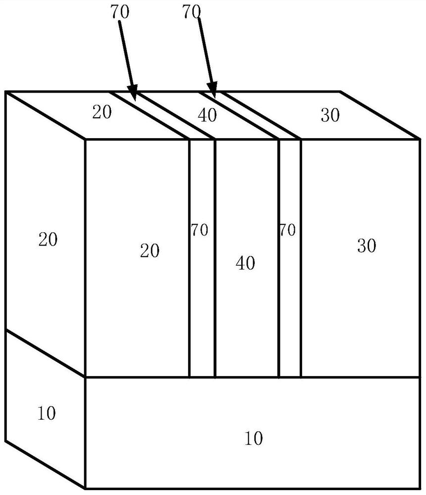
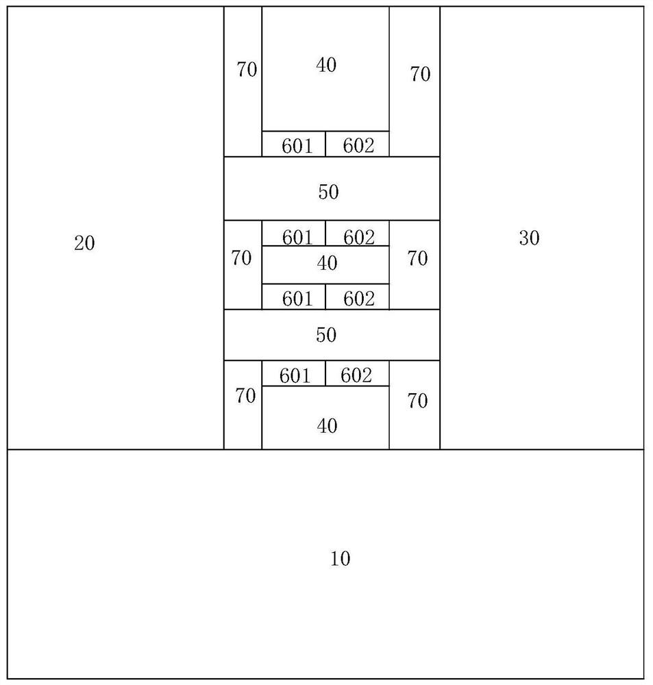
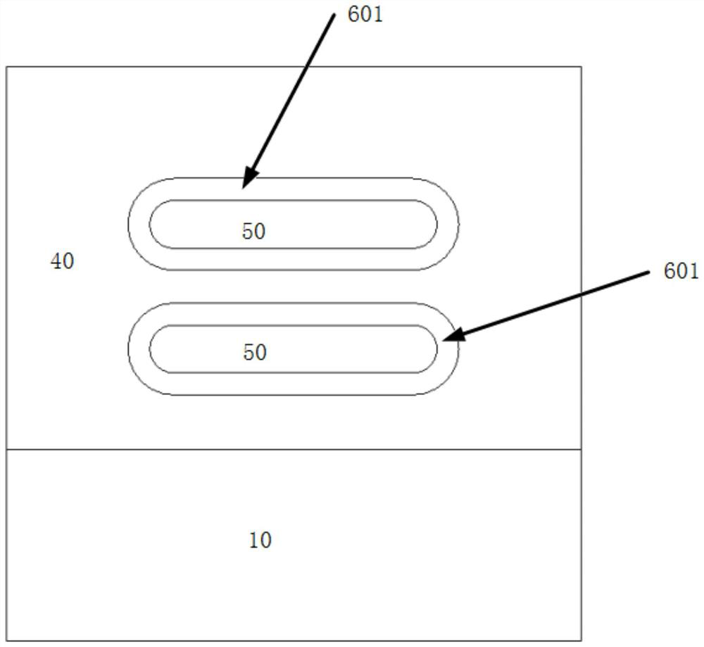
[0044] In order to reduce the short channel effect and off-state current leakage of small-sized field effect transistors and improve the electrical performance of small-sized field effect transistors, embodiments of the present invention provide a nanosheet transistor with a heterogeneous gate dielectric and a preparation method. Firstly, the nanosheet transistor with heterogeneous gate dielectric provided by the embodiment of the present invention will be described in detail. see figure 1 and figure 2 As shown, the nanosheet transistor includes: a substrate 10, a source region 20, a drain region 30, a gate material 40, and a plurality of nanosheet channel layers 50 arranged in parallel; figure 1 is the three-dimensional structure diagram of the nanosheet transistor, figure 2 is a cross-sectio...


PUM


Abstract

The invention discloses a nanosheet transistor with a heterogeneous gate medium and a preparation method. The nanosheet transistor comprises a substrate, a source region, a drain region, a gate material and a plurality of nanosheet channel layers; the gate material coats the nanosheet channel layers to form a fence structure; the source region, the fence structure and the drain region are sequentially arranged on the substrate along the channel direction; the channel direction is the direction from the source region to the drain region; heterogeneous gate dielectric layers are arranged between the adjacent surfaces of the gate material and the nanosheet channel layer and between the adjacent surfaces of the gate material and the substrate. Each heterogeneous gate dielectric layer comprises a plurality of gate dielectric materials which are continuously arranged along the channel direction, and the relative dielectric constants of the plurality of gate dielectric materials are gradually reduced along the channel direction; the source region is isolated from the gate region through a first isolation medium; the drain region is isolated from the gate region through the first isolation medium. According to the invention, the short-channel effect of the small-size field effect transistor is reduced, the off-state current leakage is reduced, and the electrical performance of the small-size semiconductor device is improved.

Description

technical field [0001] The invention belongs to the technical field of semiconductors, and in particular relates to a nanosheet transistor with a heterogeneous gate medium and a preparation method thereof. Background technique [0002] As the size of semiconductor devices gradually decreases, the short-channel effect, which has little effect on large-size devices, gradually threatens the performance of small-size devices. The short-channel effect refers to that under the condition of an applied voltage, the depletion region formed at the source-drain PN junction will shorten the channel length in a phase-changing manner. For small-sized devices, the impact of the short-channel effect becomes difficult to ignore. Moreover, due to the shortening of the channel, the electric field intensity at the drain terminal increases, making it easy for carriers to reach the drain terminal through tunneling, resulting in off-state current leakage; this phenomenon seems to reduce the barri...

Claims


Application Information

Patent Timeline
Patent Type & Authority Applications(China)
IPC IPC(8): H01L29/78H01L29/06H01L29/15H01L29/51H01L21/336
CPCH01L29/0665H01L29/158H01L29/512H01L29/66545H01L29/7856
Inventor 李高鹏
Owner 西安国微半导体有限公司
Why Eureka
Try Eureka