Carborundum semiconductor element and manufacture method for the same

A technology of semiconductor and silicon carbide, which is applied in the field of silicon carbide semiconductor components and its manufacturing, can solve the problems of high risk of mis-opening, critical voltage reduction, etc., and achieve the effect of avoiding mis-opening

Active Publication Date: 2016-07-27
SHANGHAI HESTIA POWER INC
View PDF4 Cites 3 Cited by
  • Summary
  • Abstract
  • Description
  • Claims
  • Application Information

AI Technical Summary

Problems solved by technology

[0008] However, among the currently known methods for improving and reducing the on-resistance, the most common tradeoff is to reduc

Method used


Image

  • Carborundum semiconductor element and manufacture method for the same
  • Carborundum semiconductor element and manufacture method for the same
  • Carborundum semiconductor element and manufacture method for the same

Examples


Embodiment Construction

[0035] Relating to the detailed description and technical content of the present invention, it is now described as follows in conjunction with the accompanying drawings:

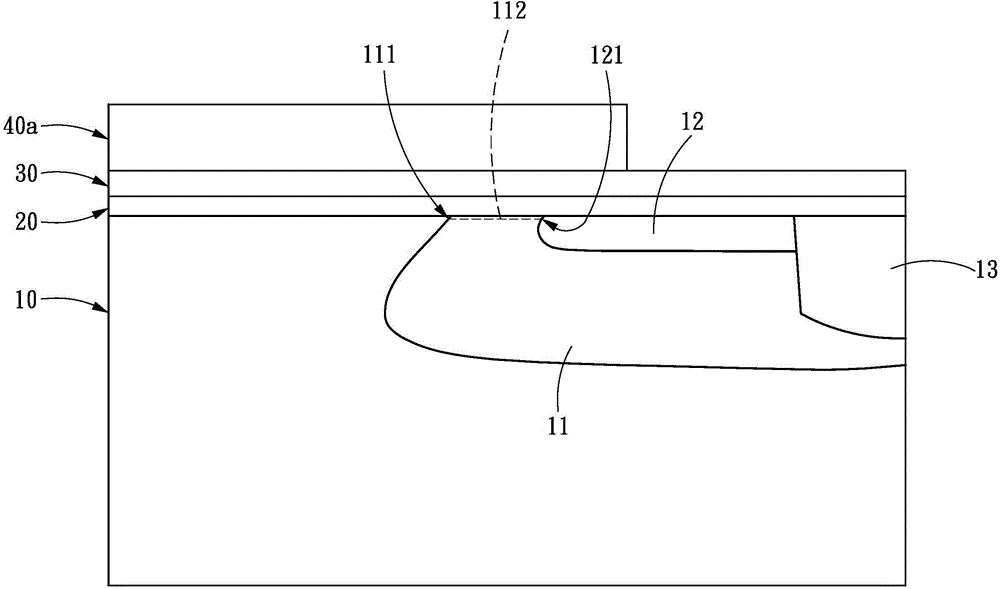
[0036] see figure 1 As shown, it is a schematic structural diagram of the first embodiment of the present invention. As shown in the figure, the present invention is a silicon carbide semiconductor element, including a first semiconductor layer 10, a second semiconductor layer 20, an insulating layer 30, an The gate electrode 40 a , a first doped region 11 , a second doped region 12 , and a third doped region 13 . The first semiconductor layer 10 has a first conductivity, and its material can be silicon carbide, and the first conductivity can be n-type, for example. The second semiconductor layer 20 is disposed on the first semiconductor layer 10, and its material can be silicon carbide, with a thickness between 0.01 μm and 0.5 μm and a thickness between 1×10 15 cm -3 to 1×10 18 cm -3 The impurity conce...


PUM

PropertyMeasurementUnit
Lengthaaaaaaaaaa
Thicknessaaaaaaaaaa

Abstract

The invention discloses a carborundum semiconductor element and a manufacture method for the same. The manufacture method comprises steps of arranging a channel control area, and enabling the channel control area to have a foreign matter concentration distribution which progressively increases from a first doped boundary, achieves a maximum value between the first doped boundary and a second doped boundary, and progressively decreases toward the second doped boundary. The manufacture method enables the carborundum semiconductor element to reduce the conduction resistor and improve the drain current without sacrificing the critical voltage.

Description

technical field [0001] The present invention relates to a semiconductor element, in particular to a silicon carbide semiconductor element and a manufacturing method thereof. Background technique [0002] In terms of the characteristics of semiconductor power components, the designed blocking voltage should have the smallest on-resistance, low reverse leakage current, and fast switching speed to reduce the conduction loss during operation. And switching loss (switchingloss). Silicon carbide (siliconcarbide, SiC) has a wide energy gap (the E of 4H-SiC g Up to 3.26eV), high critical breakdown electric field strength (2.2MV / cm) and high thermal conductivity (4.9W / cm-K), it is considered to be an excellent material for power switching components. Silicon carbide is also the only compound semiconductor that can form an oxide layer by thermal oxidation, so it can be suitable for making MOS controlled switching elements (MOS controlled switches) such as MOSFET (metal oxide semicon...

Claims


Application Information

Patent Timeline
IPC IPC(8): H01L29/78H01L21/336H01L29/41H01L29/36
Inventor 颜诚廷洪建中黄尧峯洪湘婷李傳英
Owner SHANGHAI HESTIA POWER INC
Why Eureka
Try Eureka