Method for producing a semiconductor device

一种半导体、氮化物半导体的技术,应用在半导体器件、半导体/固态器件制造、电气元件等方向,能够解决透明电极没有充分结晶等问题,达到减少光吸收、减少应变、提高半透明性和导电性的效果

Active Publication Date: 2016-07-27
TOYODA GOSEI CO LTD
View PDF3 Cites 0 Cited by
  • Summary
  • Abstract
  • Description
  • Claims
  • Application Information

AI Technical Summary

Problems solved by technology

Therefore, transparent electrodes are not sufficiently crystallized, and there is room for improved conductivity or translucency

Method used


Image

  • Method for producing a semiconductor device
  • Method for producing a semiconductor device
  • Method for producing a semiconductor device

Examples


Embodiment approach 1

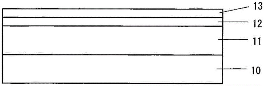
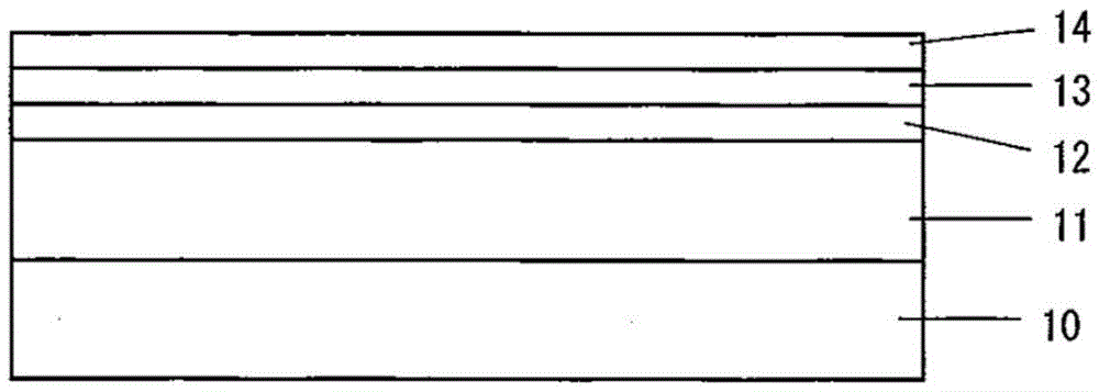
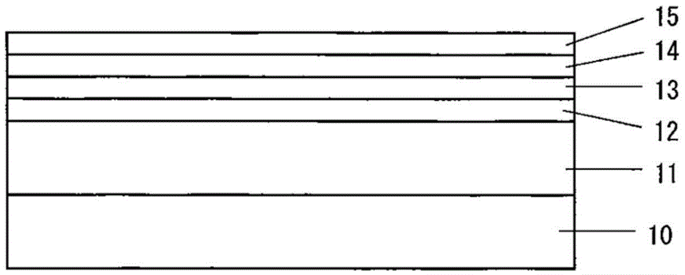
[0024] Figure 1A to Figure 1D is a schematic diagram showing a process for forming a light emitting device according to Embodiment Mode 1. FIG. figure 2 is a flowchart showing a part of the process for manufacturing the light emitting device according to Embodiment Mode 1 (before and after forming the transparent electrode 15 ). Next will refer to Figure 1A to Figure 1D with figure 2 A process for manufacturing a Group III nitride semiconductor light emitting device according to Embodiment Mode 1 will be described.

[0025] First, a sapphire substrate 10 is prepared, and heat-treated in a hydrogen atmosphere to remove impurities adhering to the surface. Next, an AlN buffer layer (not shown) is formed on the sapphire substrate 10, and an n-type layer 11, a light-emitting layer 12 and a p-type cladding layer 13 are sequentially deposited on the buffer layer by MOCVD ( Figure 1A ).

[0026] Each of n-type layer 11, light-emitting layer 12, and p-type cladding layer 13 may...


PUM

PropertyMeasurementUnit
temperatureaaaaaaaaaa

Abstract

The present invention provides a method for manufacturing a semiconductor device exhibiting improved emission efficiency by reducing strain between a p-contact layer and a transparent electrode. A transparent electrode made of IZO (zinc-doped indium oxide) is formed on the p-type contact layer by vapor deposition or sputtering. Subsequently, the p-type cladding layer and the p-type contact layer are p-type activated by indirect resistance heating, and the transparent electrode is crystallized. The heat treatment is carried out at a temperature of 700° C. under less pressure. Next, microwave heating is performed at a temperature of 100° C. to 350° C. for three minutes to thirty minutes by irradiating microwaves with a frequency of 5.8 GHz in a nitrogen atmosphere. This reduces the strain on the transparent electrode and improves the conductivity or translucency of the transparent electrode.

Description

technical field [0001] The present invention relates to a method for manufacturing a Group III nitride semiconductor device, and more particularly, to a method for reducing strain between a Group III nitride semiconductor and a transparent electrode. Background technique [0002] In a conventional method for manufacturing a Group III nitride semiconductor light emitting device, after forming a transparent electrode made of a material such as ITO and IZO on a p-type layer, heat treatment is performed to crystallize the transparent electrode. This improves the conductivity of the transparent electrode, and reduces light absorption. [0003] Japanese Published (kokai) Patent Application No. 2014-154584 describes heating the p-type layer and the transparent electrode, preferably by microwave heating, in order to activate the p-type layer and simultaneously crystallize the transparent electrode. [0004] However, as crystallization of the transparent electrode by heat treatment ...

Claims


Application Information

Patent Timeline
Patent Type & Authority Applications(China)
IPC IPC(8): H01L33/00H01L21/324H01L33/36
CPCH01L33/42H01L33/32H01L2933/0016H01L21/324H01L33/0075H01L33/36
Inventor 户谷真悟中内润
Owner TOYODA GOSEI CO LTD
Why Eureka
Try Eureka