Growing method for high-surface-quality silicon carbide epitaxial layer
A technology of high-quality silicon carbide and growth methods, which is applied in electrical components, semiconductor/solid-state device manufacturing, circuits, etc., can solve problems such as device leakage and failure, and achieve the effect of reducing triangular defects and avoiding the formation of step bunching morphology.
- Summary
- Abstract
- Description
- Claims
- Application Information
AI Technical Summary
Problems solved by technology
Method used
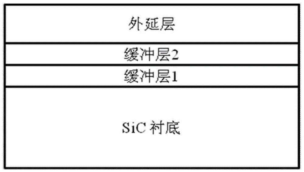
Image

Examples
Embodiment 1
[0025] A method for growing a high-surface-quality silicon carbide epitaxial layer provided in a SiC chemical vapor deposition epitaxial system includes the following steps:
[0026] 1) Select a silicon carbide substrate with a silicon surface that is 4° to the direction, and place the substrate on a graphite base with a tantalum carbide coating in the reaction chamber of the SiC epitaxy system;
[0027] 2) The temperature of the system is raised to 1450°C, and the set pressure is 100mbar, under hydrogen (H 2 ) flow rate of 80L / min, maintain the temperature of the reaction chamber for 5 minutes, and carry out pure hydrogen (H 2 ) etching;
[0028] 3) Introduce a small amount of hydrogen chloride (HCl) into the reaction chamber to assist substrate etching, HCl / H 2 The flow ratio is set to 0.01%;
[0029] 4) Continue to raise the temperature, maintain the temperature for 5 minutes after reaching 1660°C, keep the flow rate of hydrogen chloride (HCl) constant, and continue to ...
PUM
 Abstract
Description
Claims
Application Information
 - R&D
- Intellectual Property
- Life Sciences
- Materials
- Tech Scout
- Unparalleled Data Quality
- Higher Quality Content
- 60% Fewer Hallucinations
Browse by: Latest US Patents, China's latest patents, Technical Efficacy Thesaurus, Application Domain, Technology Topic, Popular Technical Reports.
© 2025 PatSnap. All rights reserved.Legal|Privacy policy|Modern Slavery Act Transparency Statement|Sitemap|About US| Contact US: help@patsnap.com