A liquid crystal-based imaging detection chip with an addressable tomographic field of view

A liquid crystal and imaging technology, applied in the field of imaging detection, can solve problems such as slow response, inability to perform image inspection, limited scalability, etc., and achieve the effect of flexible control mode

Active Publication Date: 2018-11-30
HUAZHONG UNIV OF SCI & TECH
View PDF4 Cites 0 Cited by
  • Summary
  • Abstract
  • Description
  • Claims
  • Application Information

AI Technical Summary

Problems solved by technology

[0003] At present, with the continuous and rapid development of microelectronics technology, the array size of photosensitive chips is still expanding. Laboratory-level single-chip scientific research products have exceeded the level of 100 million pixels, and the size of photosensitive elements has shrunk to the sub-micron scale. This progress In terms of further improving the imaging clarity, radiation resolution, and expanding the radiation response range based on the objective lens or light converging ability, it will have a significant improvement and even significantly enhance the imaging detection efficiency, but there are institutional constraints on the tomographic imaging of the scene. still exist, thereby showing the deficiency of insufficient capacity
The key problems are: (1) the depth of focus of the existing imaging optical system is extremely limited, and the increment of depth of focus that can be obtained through expensive means is not enough to support the significant expansion of the number of clear layers; (2) the mechanical The optical steady-state transition period under focusing is long, and the response is relatively slow, which is not suitable for dynamic or rapidly changing processes and image information capture of fast-moving targets; Divide or determine the clear layer positions of relatively stable or slowly changing scenes, it is difficult to perform fine tomography and addressable accurate inspection of the field of view; (4) Based on the architecture of electronically controlled deformable microlens array and photosensitive chip integration Adjustable focus operation, due to the sequence of structural deformation and the inertia of shape changes, it is only suitable for stable or slowly changing scenes and cannot perform fast jump image inspection; (5) Based on multi-focus long-diffraction microlens arrays and photosensitive chips Coupling to perform adjustable-focus imaging detection, the essence is still to roughly divide the field of view, and there are also problems such as the inability to finely layer the field of view and perform accurate inspection; (6) Based on the multi-focus long-refraction microlens array coupled Chip-matched to perform variable-focus imaging detection, similar issues exist with multi-focal-length diffractive microlenses

Method used


Image

  • A liquid crystal-based imaging detection chip with an addressable tomographic field of view
  • A liquid crystal-based imaging detection chip with an addressable tomographic field of view
  • A liquid crystal-based imaging detection chip with an addressable tomographic field of view

Examples


Embodiment Construction

[0027] In order to make the object, technical solution and advantages of the present invention clearer, the present invention will be further described in detail below in conjunction with the accompanying drawings and embodiments. It should be understood that the specific embodiments described here are only used to explain the present invention, not to limit the present invention. In addition, the technical features involved in the various embodiments of the present invention described below can be combined with each other as long as they do not constitute a conflict with each other.

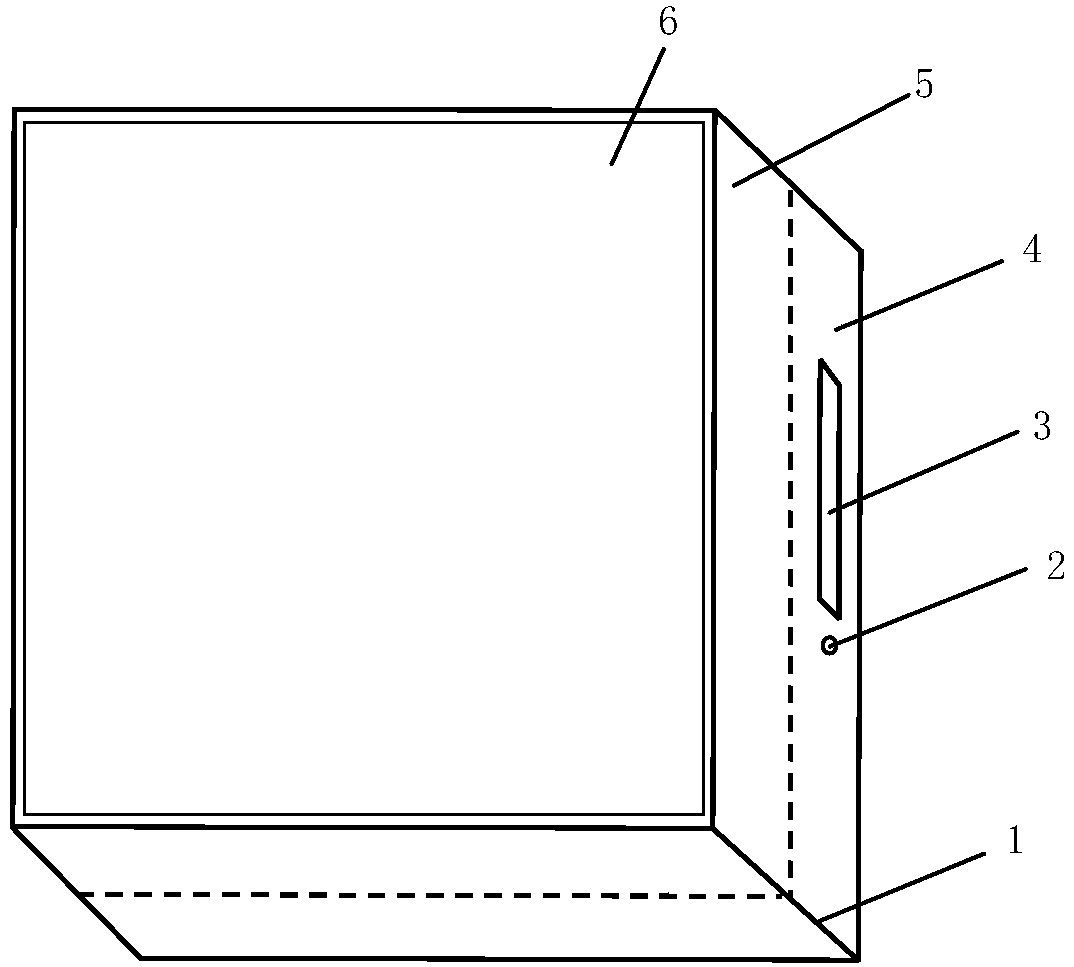
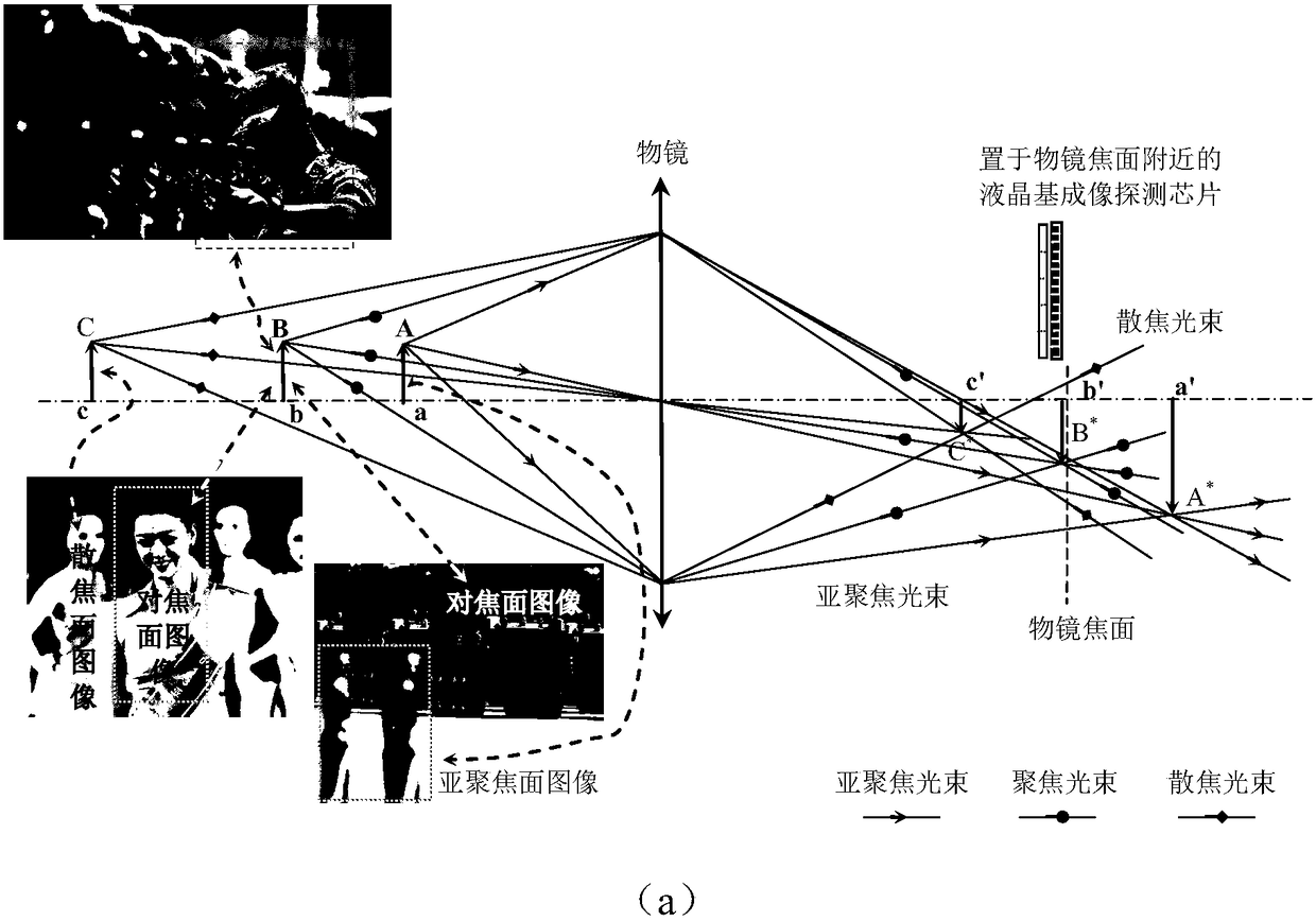
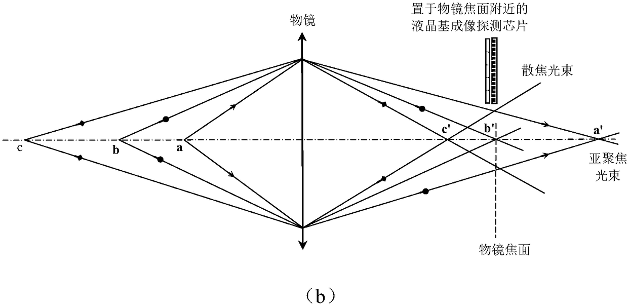
[0028] figure 1 It is a structural schematic diagram of a liquid crystal-based imaging detection chip with an addressable tomographic field of view according to an embodiment of the present invention. As shown in the figure, the area array electronically controlled liquid crystal imaging microlens 5 and the area array photosensitive detector 4 are arranged coaxially and sequentially coupled and...


PUM


Abstract

The invention discloses a liquid crystal based imaging detection chip of an addressable chromatographic field. The chip comprises a planar array electric control imaging microlens and a planar array light sensitive detector, a unit electric control imaging microlens further compresses a compression light field, formed by an objective lens, of an object in a gathering manner, the mean-square amplitude of the signal voltage loaded on the planar array electric control imaging microlens is modulated, the light gathering capability of the unit electric control imaging microlens is modulated, a target focusing plane which is determined by the objective lens and the unit electric control imaging microlens together is further modulated, a target layer capable of imaging clearly is changed in the depth direction, and addressable chromatographic roll call in the depth direction of the imaging field is executed. The chip is easy to couple with other functional optical, photoelectric and electronic structures, and can be easily inserted into a routine imaging optical path to replace a traditional photosensitive chip to execute imaging detection of the addressable chromatographic field.

Description

technical field [0001] The invention belongs to the field of imaging detection technology, and more specifically relates to a liquid crystal-based imaging detection chip with an addressable tomographic field of view. The local imaging field of view is realized through an area array electronically controlled liquid crystal imaging microlens and an area array photosensitive detector. Field addressable tomography. Background technique [0002] So far, imaging detection technology based on large area array photosensitive chips has been widely used. With the popularization of smart phones, small / miniaturized image structures with a scale of tens of millions of pixels have entered the era of personal consumption. The pursuit of efficiency has shown the consumption direction of only better and stronger. Generally speaking, the existing conventional imaging detection system is based on the objective lens or imaging optical system, which compresses the target light field on a large ...

Claims


Application Information

Patent Timeline
Patent Type & Authority Patents(China)
IPC IPC(8): H01L27/146
CPCH01L27/14603
Inventor 张新宇信钊炜魏东袁莹彭莎张波吴勇王海卫谢长生
Owner HUAZHONG UNIV OF SCI & TECH
Why Eureka
Try Eureka