Double-side growth four-junction solar cell with reflecting layer and preparation method thereof

A solar cell and double-sided growth technology, applied in the field of solar photovoltaics, can solve the problems of small minority carrier diffusion length, low short-circuit current of GaInNAs cells, and inability to effectively collect photogenerated carriers, so as to improve photoelectric conversion performance and reduce costs Effect

Inactive Publication Date: 2016-08-03
ZHONGSHAN DEHUA CHIP TECH CO LTD
View PDF4 Cites 17 Cited by
  • Summary
  • Abstract
  • Description
  • Claims
  • Application Information

AI Technical Summary

Problems solved by technology

[0005] However, due to the high background carrier concentration of GaInNAs materials, this will make the minority carrier diffusion length smaller
In this case, if the GaInNAs material grows too thick, it cannot achieve the effect of effectively collecting photogenerated carriers; on the contrary, if the GaInNAs material grows too thin, it cannot fully absorb the photons of the corresponding wavelength band, and the consequence is the short-circuit current of the GaInNAs battery. Low

Method used


Image

  • Double-side growth four-junction solar cell with reflecting layer and preparation method thereof
  • Double-side growth four-junction solar cell with reflecting layer and preparation method thereof
  • Double-side growth four-junction solar cell with reflecting layer and preparation method thereof

Examples


Embodiment Construction

[0041] The present invention will be further described below in conjunction with specific embodiments.

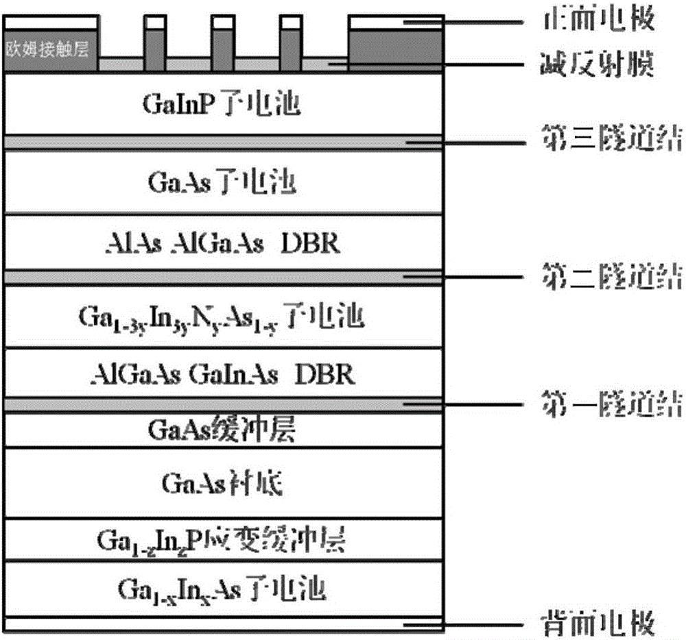
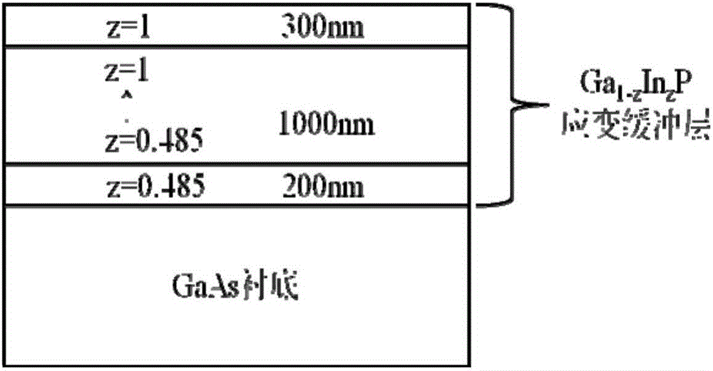
[0042] Such as figure 1 As shown, the double-sided growth four-junction solar cell of this embodiment includes a GaAs substrate. The GaAs substrate is a double-sided polished n-type GaAs single wafer using metal organic chemical vapor deposition (MOCVD) technology. On the upper surface of the 4-inch GaAs substrate, a GaAs buffer layer, first tunnel junction, AlGaAs / GaInAsDBR reflective layer, GaInNAs sub-cell, second tunnel junction, AlAs / AlGaAsDBR reflective layer, The GaAs sub-cell, the third tunnel junction, the GaInP sub-cell, the ohmic contact layer, the anti-reflection film, and the front electrode are sequentially arranged with GaAs on the bottom surface of the GaAs substrate. 1-z In z P strain buffer layer, Ga 1-x In x As sub-cell and back electrode, the AlGaAs / GaInAsDBR reflective layer is used to reflect long-wave photons, and the AlAs / AlGaAsDBR reflective layer is us...


PUM


Abstract

The invention discloses a double-side growth four-junction solar cell with a reflecting layer and a preparation method thereof, and the solar cell comprises a GaAs substrate; the GaAs substrate is an n-type GaAs single-crystal slice that is polished in two sides; a GaAs buffer layer, a first tunnel junction, a AlGaAs/GaInAs DBR reflecting layer, a GaInNAs sub-cell, a second tunnel junction, a AlAs/AlGaAs DBR reflecting layer, a GaAs sub-cell, a third tunnel junction, a GaInP sub-cell, an ohmic contact layer, an antireflection coating, and a front electrode grow on the upper surface of the GaAs substrate from top to bottom; a Ga1-zInzP strain buffer layer, a Ga1-xInxAs sub-cell and a back electrode are provided on the lower surface of the GaAs substrate in order. According to the invention, photon absorption efficiency can be raised; at the same time, the advantages of the four-junction solar cell can play their roles; the integral open-circuit voltage and a fill factor of the GaAs multi-junction cell can be raised; and the photoelectric conversion efficiency of the cell can be improved finally.

Description

Technical field [0001] The invention relates to the technical field of solar photovoltaics, in particular to a double-sided growth four-junction solar cell with a reflective layer and a preparation method thereof. Background technique [0002] At present, traditional gallium arsenide multi-junction solar cells are widely used in concentrated photovoltaic power generation (CPV) systems and space power systems because their conversion efficiency is significantly higher than that of crystalline silicon cells. The mainstream structure of gallium arsenide multi-junction battery is GaInP / GaInAs / Ge triple-junction solar cell composed of GaInP, GaInAs and Ge sub-cells. The battery structure maintains lattice matching as a whole, and the band gap structure is 1.85 / 1.40 / 0.67eV. However, for the solar spectrum, due to the large band gap gap between the GaInAs sub-cell and the Ge sub-cell, the band gap combination of this triple junction cell is not optimal. The solar spectrum absorbed by th...

Claims


Application Information

Patent Timeline
Patent Type & Authority Applications(China)
IPC IPC(8): H01L31/0687H01L31/0216H01L31/0304H01L31/18
CPCH01L31/02168H01L31/03046H01L31/0687H01L31/1844Y02E10/544Y02P70/50
Inventor 刘雪珍杨翠柏王雷吴波黄珊珊陈丙振张小宾张杨
Owner ZHONGSHAN DEHUA CHIP TECH CO LTD
Why Eureka
Try Eureka