Enhanced GaN-based high electron mobility transistor and preparation method thereof

A high electron mobility, transistor technology, applied in the field of microelectronics, can solve the problems of low gate threshold voltage etching damage, restricting the popularization and application of P-GaN capping layer technology, and poor control of etching depth, etc. Gate Threshold Voltage, Overcoming Etch Damage Difficulty Controlling Effects

Active Publication Date: 2016-08-10
INST OF MICROELECTRONICS CHINESE ACAD OF SCI
View PDF4 Cites 12 Cited by
  • Summary
  • Abstract
  • Description
  • Claims
  • Application Information

AI Technical Summary

Problems solved by technology

[0004] The gate threshold voltage of the enhanced GaN-based high electron mobility transistor formed by the preparation process of the P-GaN capping layer (a) generally does not exceed 2V; The etch depth and damage of P-Al(In,Ga)N are difficult to control, which seriously restricts the popularization and application of P-GaN capping layer technology in GaN-based power electronics
When the gate groove etching technology (b) is used, the 2DEG can be completely dep...

Method used


Image

  • Enhanced GaN-based high electron mobility transistor and preparation method thereof
  • Enhanced GaN-based high electron mobility transistor and preparation method thereof
  • Enhanced GaN-based high electron mobility transistor and preparation method thereof

Examples


Embodiment Construction

[0021] In order to make the purpose, technical solutions and advantages of the embodiments of the present invention clearer, the technical solutions in the embodiments of the present invention will be clearly and completely described below in conjunction with the drawings in the embodiments of the present invention. Obviously, the described embodiments It is only some embodiments of the present invention, but not all embodiments. Based on the embodiments of the present invention, all other embodiments obtained by persons of ordinary skill in the art without making creative efforts belong to the protection scope of the present invention.

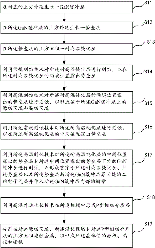
[0022] The invention provides a preparation method of an enhanced GaN-based high electron mobility transistor, such as figure 1 As shown, the method includes:

[0023] S11. Epitaxially grow a GaN buffer layer on the substrate.

[0024] S12. Epitaxially growing a barrier layer on the GaN buffer layer.

[0025] Optionally, the barrier layer ...


PUM


Abstract

The invention provides a GaN-based enhanced high electron mobility transistor and a preparation method thereof. The transistor comprises a substrate GaN buffer layer, a barrier layer and a passivation layer from the bottom to the top. The transistor further comprises a gate groove which runs through the high temperature resistance passivation layer, the barrier layer and a two-dimensional electron gas layer on the interface of the barrier layer and the GaN buffer layer and extends into the GaN buffer layer. A P-type gate dielectric layer grows in the gate groove. The gate of the transistor is located above the P-type gate dielectric layer. The source and the drain of the transistor are respectively located on both sides of the GaN buffer layer. According to the invention, higher gate threshold voltage can be acquired; and the defects of difficult control of etching damage and damaged conduction channel carrier mobility caused by over-etching can be overcome.

Description

technical field [0001] The invention relates to the technical field of microelectronics, in particular to an enhanced GaN-based high electron mobility transistor and a preparation method thereof. Background technique [0002] With the development of high-voltage switches and high-speed radio frequency circuits, enhancement-mode GaN-based high electron mobility transistors (High ElectronMobility Transistor, HEMT) have become another research focus. The enhanced GaN-based HEMT can only have a working current when a positive gate voltage is applied, which can greatly expand its application in low-power digital circuits. In order to obtain a higher gate threshold voltage, there are currently two mainstream methods for preparing enhancement-mode GaN-based high electron mobility transistors: a) growing a layer on the traditional Al(In,Ga)N / GaN heterostructure The P-GaN cap layer uses the space charge effect of the PN junction to deplete the two-dimensional electron gas (2DEG) to ...

Claims


Application Information

Patent Timeline
IPC IPC(8): H01L29/778H01L29/06H01L21/335
CPCH01L29/0603H01L29/66431H01L29/778
Inventor 黄森刘新宇王鑫华魏珂
Owner INST OF MICROELECTRONICS CHINESE ACAD OF SCI
Why Eureka
Try Eureka