Fabrication process of crystalline silicon solar cell

A solar cell and manufacturing process technology, applied in sustainable manufacturing/processing, final product manufacturing, semiconductor/solid-state device manufacturing, etc., can solve the problem of not being able to cover the bottom of the fleece layer, so as to improve photoelectric conversion efficiency, increase production capacity, and reduce cost effect

Active Publication Date: 2016-08-17
JIANGSU MICROVIA NANO EQUIP TECH CO LTD
View PDF12 Cites 26 Cited by
  • Summary
  • Abstract
  • Description
  • Claims
  • Application Information

AI Technical Summary

Problems solved by technology

like figure 2 As shown, the so-called "pyramid" formed by conventional wet acid texturing has a small aspect ratio, and the PECVD anti-reflection layer can be directly formed on the textured surface; however, for the textured surface with high aspect ratio formed by RIE etching, traditional The PECVD anti-reflection layer cannot cover the bottom of the fleece layer, causing defects

Method used


Image

  • Fabrication process of crystalline silicon solar cell
  • Fabrication process of crystalline silicon solar cell
  • Fabrication process of crystalline silicon solar cell

Examples


Embodiment 1

[0068] Example 1 Preparation of common PERC battery anti-reflection layer and ALD passivation layer process

[0069] Using the present invention to firstly prepare the ordinary PERC battery structure and the anti-reflection layer, and then carry out the process of ALD technology double-sided coating passivation layer, using different reaction chambers and process parameters, SiN can be prepared x / SiO 2 / Al 2 o 3 / SiN x Composite structure, the implementation of specific process parameters and the prepared composite structure are as follows:

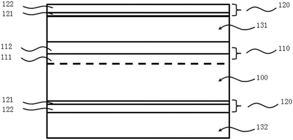
[0070] Table 2 Preparation of SiN x / SiO 2 / Al 2 o 3 / SiN x Composite structure( Figure 3A ) of the parameters of the specific embodiment, the specific process see Figure 4A

[0071]

[0072] Note: step 121 and step 122 perform double-sided coating at the same time in the same cavity, and step 131 and step 132 choose different cavities for PEALD or PECVD single-sided coating according to the actual situation.

[0073] Wh...

Embodiment 2

[0080] Example 2 Process for preparing ALD passivation layer and PEALD antireflection layer / protective layer of common PERC battery

[0081] Using the present invention to first prepare the double-sided coating of the ALD passivation layer of the PERC battery structure, and then perform the process of PEALD or PECVD anti-reflection layer and passivation layer, and use the same ALD / PEALD reaction chamber and process parameters to prepare SiN x / SiO 2 / Al 2 o 3 / SiN x Composite structure, the implementation of specific process parameters and the prepared composite structure are as follows:

[0082] Table 5 Preparation of SiN x / SiO 2 / Al 2 o 3 / SiN x Composite structure( Figure 3B ) of the specific embodiment of the parameters (using the same ALD / PEALD reaction chamber, the specific process is shown in Figure 4B-1 )

[0083]

[0084] Note: step 121 and step 122 perform double-sided coating at the same time in the same cavity, and step 130 performs PEALD double-si...

Embodiment 3

[0085] Example 3 Process for preparing ALD passivation layer and PEALD / PECVD antireflection layer / protective layer of common PERC battery

[0086] Using the present invention to first prepare the ALD passivation layer double-sided coating of the PERC battery structure, and then perform the process of PEALD or PECVD anti-reflection layer and passivation layer, and use different ALD / PEALD / PECVD reaction chambers and process parameters to prepare SiN x / SiO 2 / Al 2 o 3 / SiN x Composite structure, the implementation of specific process parameters and the prepared composite structure are as follows:

[0087] Table 6 Preparation of SiN x / SiO 2 / Al 2 o 3 / SiN x Composite structure( Figure 3B ) of the parameters of specific embodiments (using different ALD / PEALD / PECVD reaction chambers, see the specific process flow Figure 4B-2 )

[0088]

[0089] Note: Step 120 performs double-sided coating in the ALD chamber at the same time, and step 130 performs double-sided coati...


PUM

PropertyMeasurementUnit
thicknessaaaaaaaaaa
thicknessaaaaaaaaaa
thicknessaaaaaaaaaa

Abstract

The invention relates to the field of fabrication of a solar cell, in particular to a surface passivation and anti-reflection technology of crystalline silicon cell for improving photoelectric conversion efficiency. Aiming at the existing cell technology process flow, nanometer lamination of a material such as SiO2, Al2O3 and SiNx and a composite material are fabricated by atomic layer deposition and plasma atomic layer deposition, passivation layer plating is carried out on the front surface and the back surface of the crystalline silicon cell, so that the minority carrier lifetime is prolonged, and the photoelectric conversion efficiency of the cell is improved; and SiNx anti-reflection layer plating can be continuously carried out after passivation layer plating, so that passivation and anti-reflection processes can be integrated in the same flow, the cost is reduced, and the yield is improved. The fabrication method is particularly and suitably used for combining with a black silicon technology, and multiple processes are avoided; and moreover, for a double-sided battery, the fact that double-sided passivation is carried out by using the fabrication method is a necessary choice.

Description

technical field [0001] The invention relates to the field of solar cell manufacturing, in particular to the surface passivation and anti-reflection technology of crystalline silicon cells for improving photoelectric conversion efficiency. Background technique [0002] High-efficiency crystalline silicon cells are an important development trend of the photovoltaic industry. In order to maximize the photoelectric conversion efficiency of crystalline silicon cells, surface texturing and passivation processes are necessary means for high-efficiency cell manufacturing, such as passivated emitter back cells, that is, PERC cell technology has attracted much attention. And the battery production technology is also continuously improving and improving. Among them, black silicon technology combined with back passivation technology can achieve a conversion efficiency of more than 20%. [0003] Different from ordinary acid texturing, the RIE etching black silicon technology, which is ...

Claims


Application Information

Patent Timeline
Patent Type & Authority Applications(China)
IPC IPC(8): H01L31/18H01L21/02
CPCH01L21/02164H01L21/0217H01L21/02178H01L21/022H01L21/02274H01L21/0228H01L31/1804H01L31/1868Y02E10/547Y02P70/50
Inventor 黎微明李翔胡彬王燕清
Owner JIANGSU MICROVIA NANO EQUIP TECH CO LTD
Why Eureka
Try Eureka