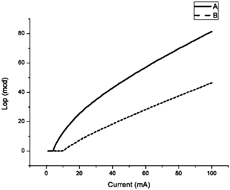
A kind of preparation method of LED epitaxial wafer that improves luminous efficiency
A technology for LED epitaxial wafers and luminous efficiency, which is applied to semiconductor devices, electrical components, circuits, etc., can solve the problems of cumbersome and complicated process steps, unfavorable promotion and application, and high cost required to achieve simple process steps, improve luminous efficiency, low cost effect
- Summary
- Abstract
- Description
- Claims
- Application Information
AI Technical Summary
Problems solved by technology
Method used
Image
Examples
preparation example Construction
[0029] For a kind of LED epitaxial wafer preparation method that improves luminous efficiency of the present invention, its concrete steps comprise:
[0030] A, epitaxially growing a buffer layer on a sapphire substrate;
[0031] B. epitaxially growing an n-type gallium nitride layer on the buffer layer;
[0032] C. Epitaxial growth of multiple quantum well layers on the n-type gallium nitride layer;
[0033] D. Epitaxially grow at least two isolation layers from bottom to top on the multi-quantum well layer; wherein, the growth temperature of the at least two isolation layers is gradually increased according to the epitaxial growth sequence of the at least two isolation layers from first to last Big;
[0034] E. Epitaxially growing a p-type gallium nitride layer on the last epitaxially grown isolation layer. For example, the number of layers of the epitaxially grown isolation layer is 4, that is, the first isolation layer, the second isolation layer, the third isolation la...
specific Embodiment
[0049] The specific steps of a method for preparing LED epitaxial wafers that improve invention efficiency include:
[0050] S1, on the sapphire substrate (Al 2 o 3 ) on the sapphire substrate (Al 2 o 3 ) for nitriding treatment on the surface;
[0051] S2. Using a two-step growth method on a sapphire substrate (Al 2 o 3 ) epitaxial growth buffer layer (GaN);
[0052] The step S2 specifically includes: first low-temperature nucleation, and then high-temperature epitaxial growth of a rough layer (1020°C consistent with the annealing temperature) and a recovery layer (1065°C);
[0053] S3. Epitaxial growth of an n-type layer (GaN:Si) on the buffer layer (GaN), that is, an n-type gallium nitride layer doped with Si; wherein, the growth temperature of the n-type layer (GaN:Si) is 1050°C , the growth rate is controlled to be 2.6 μm / h, and the thickness is 2.6 μm to 2.7 μm;
[0054] S4. Epitaxially growing multiple quantum well layers (InGaN / GaN) on the above n-type layer (GaN...
PUM
| Property | Measurement | Unit |
|---|---|---|
| thickness | aaaaa | aaaaa |
| temperature | aaaaa | aaaaa |
| temperature | aaaaa | aaaaa |
Abstract
Description
Claims
Application Information
 - R&D
- Intellectual Property
- Life Sciences
- Materials
- Tech Scout
- Unparalleled Data Quality
- Higher Quality Content
- 60% Fewer Hallucinations
Browse by: Latest US Patents, China's latest patents, Technical Efficacy Thesaurus, Application Domain, Technology Topic, Popular Technical Reports.
© 2025 PatSnap. All rights reserved.Legal|Privacy policy|Modern Slavery Act Transparency Statement|Sitemap|About US| Contact US: help@patsnap.com


