Metal-chalcogen semiconductor material as well as preparation method and application thereof

A semiconductor and chalcogen technology, applied in the field of metal-chalcogen semiconductor materials, and its preparation, can solve the problems of difficult to achieve large-scale industrial production, poor controllability, complex nanocrystal preparation process, etc., to achieve thermoelectric value and energy conversion high efficiency effect

Inactive Publication Date: 2016-09-07
深圳热电新能源科技有限公司
View PDF10 Cites 3 Cited by
  • Summary
  • Abstract
  • Description
  • Claims
  • Application Information

AI Technical Summary

Problems solved by technology

However, the preparation process of such metal-chalcogenide semiconductor nanocrystals is relatively complex or poorly controllable or difficult to achieve large-scale industrial production.

Method used


Image

  • Metal-chalcogen semiconductor material as well as preparation method and application thereof
  • Metal-chalcogen semiconductor material as well as preparation method and application thereof
  • Metal-chalcogen semiconductor material as well as preparation method and application thereof

Examples


Embodiment 1

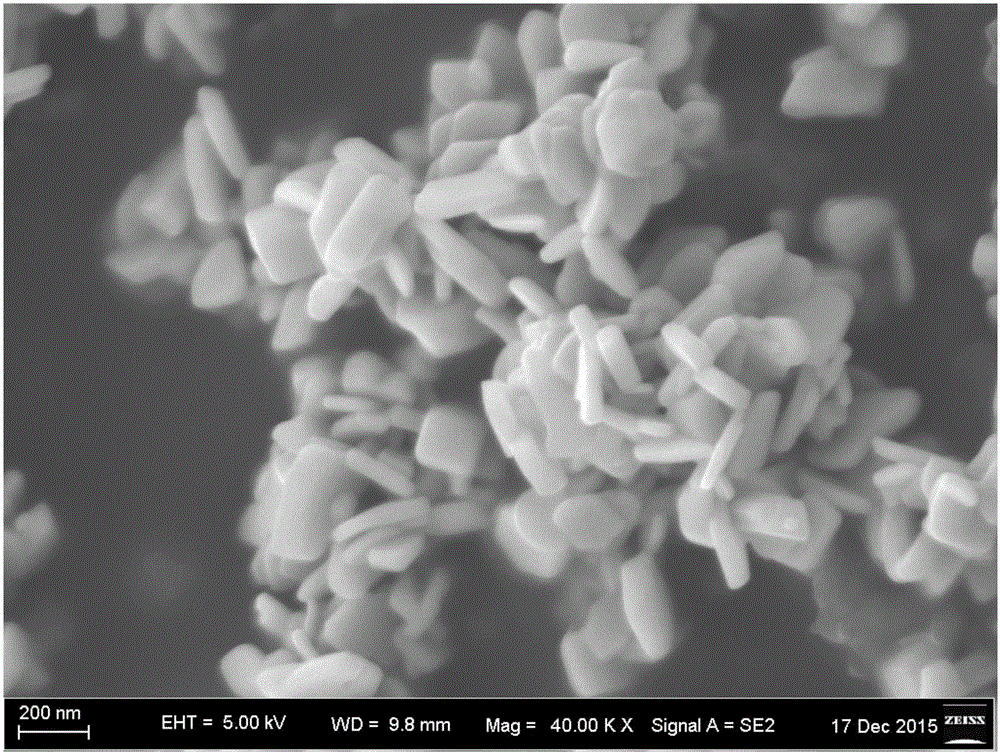
[0067] A kind of SnSe ultra-thin nanosheet, its scanning electron microscope picture is as follows figure 1 As shown, it can be seen from the figure that the size of the SnSe ultra-thin nanosheet is 50-200 nanometers, and the thickness is 1-10 nanometers.

[0068] Its preparation method comprises the following steps:

[0069] (1) Add 4g of Se elemental powder and 8g of SnCl in the reaction vessel 2 Powder and 30mL of oleylamine are mixed to obtain a precursor solution;

[0070] (2) Under stirring conditions, add 50 mL of hexamethyldisilamine (HMDS) to the precursor solution, heat to 150 ° C, and carry out hydrothermal reaction under stirring conditions for 8 hours to obtain the reaction product;

[0071] (3) The reaction product is centrifuged at 10000rpm for 10min. After the centrifugation ends, the supernatant is removed, and the precipitate is washed several times with ethanol and acetone mixture (mixed in any proportion) or acetone. suspended in water or other organic s...

Embodiment 2

[0074] A SnSe ultrathin nanosheet, the SnSe ultrathin nanosheet has a size of 50-200 nanometers and a thickness of 1-10 nanometers.

[0075] Its preparation method comprises the following steps:

[0076] (1) Add 0.001g of Se elemental powder and 10g of SnCl to the reaction vessel 2 The powder and 10mL of oleylamine are mixed to obtain a precursor solution;

[0077] (2) Add 0.01 mL of hexamethyldisilazine (HMDS) to the precursor solution under stirring conditions, heat to 80°C, and carry out hydrothermal reaction under stirring conditions for 12 hours to obtain the reaction product;

[0078] (3) The reaction product is centrifuged at 15000rpm for 30min. After the centrifugation ends, the supernatant is removed, and the precipitate is washed several times with ethanol and acetone mixture (mixed in any proportion) or acetone. suspended in water or other organic solvents).

[0079] After calculation, the yield of the SnSe ultra-thin nanosheets is 92%.

Embodiment 3

[0081] A SnSe ultrathin nanosheet, the SnSe ultrathin nanosheet has a size of 50-200 nanometers and a thickness of 1-10 nanometers.

[0082] Its preparation method comprises the following steps:

[0083] (1) Add 10g of Se elemental powder and 0.001g of SnCl to the reaction vessel 2 The powder and 1000mL of oleylamine are mixed to obtain a precursor solution;

[0084] (2) Add 100 mL of hexamethyldisilamine (HMDS) to the precursor solution under stirring conditions, heat to 300° C., and carry out hydrothermal reaction under stirring conditions for 12 hours to obtain the reaction product;

[0085] (3) The reaction product is centrifuged at 1000rpm for 5min. After the centrifugation ends, remove the supernatant, and the precipitate is washed several times with ethanol and acetone mixture (mixed in any proportion) or acetone. suspended in water or other organic solvents).

[0086] After calculation, the yield of the SnSe ultra-thin nanosheets is 92%.


PUM

PropertyMeasurementUnit
Thicknessaaaaaaaaaa

Abstract

The invention provides a metal-chalcogen semiconductor material as well as a preparation method and application thereof. The metal-chalcogen semiconductor material comprises a metal-chalcogen semiconductor crystal, wherein at least one of the three-dimension scales of the metal-chalcogen semiconductor crystal is 1-100 nanometers, the metal-chalcogen semiconductor crystal is a nano sheet or a nano cube, the nano sheet has an atomic-scale thickness, and an exposed crystal face of the nano cube is a {100} crystal face. The metal-chalcogen semiconductor material belongs to nano semiconductor crystal materials, is uniform in grain size, controllable in shape and size, and good in performance, and the preparation method of the metal-chalcogen semiconductor material needs a small amount of raw material species, is mild in reaction condition, high in yield, and suitable for industrial application.

Description

technical field [0001] The invention belongs to the technical field of semiconductor nanomaterials and new energy, and relates to a metal-chalcogenide semiconductor material, its preparation method and application. Background technique [0002] Metal-chalcogenide semiconductors have excellent energy conversion and storage functions, and are widely used in human production, life and scientific research, while the energy conversion and storage properties of metal-chalcogenide semiconductor nanocrystals are more prominent. [0003] In recent years, the preparation and application of metal-chalcogenide semiconductor nanocrystals have attracted people's attention. Through a simple and green process, metal-chalcogenide semiconductor nanomaterials with controllable morphology, good monodispersity, high yield and excellent performance have been synthesized. It has always been the focus of people's research. [0004] CN 104418311A discloses a Cu 2-x The preparation method of Se nan...

Claims


Application Information

Patent Timeline
IPC IPC(8): C01B19/04B82Y30/00B82Y40/00
CPCB82Y30/00B82Y40/00C01B19/04C01P2004/03C01P2004/20C01P2004/38C01P2004/64
Inventor 何佳清谢晓滨林京洋冯丹
Owner 深圳热电新能源科技有限公司
Why Eureka
Try Eureka