
Method using dipole moment model to inverse PCB circuit electromagnetic field

A technology of dipole moment and electromagnetic field, which is applied in the field of inversion of electromagnetic field of PCB circuit by using dipole moment model, which can solve the problem that the electromagnetic field distribution of PCB circuit board is difficult to obtain and other problems

Active Publication Date: 2016-09-07
BEIHANG UNIV
View PDF5 Cites 7 Cited by
  • Summary
  • Abstract
  • Description
  • Claims
  • Application Information

AI Technical Summary

Problems solved by technology

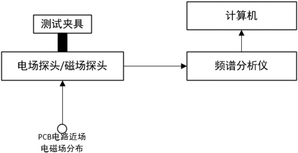
[0004] In order to solve the problem that the distribution of the electromagnetic field generated by the PCB circuit board is difficult to obtain, the present invention proposes a method for inverting the electromagnetic field of the PCB circuit using a dipole moment model

Method used


Image

  • Method using dipole moment model to inverse PCB circuit electromagnetic field
  • Method using dipole moment model to inverse PCB circuit electromagnetic field
  • Method using dipole moment model to inverse PCB circuit electromagnetic field

Examples


Embodiment

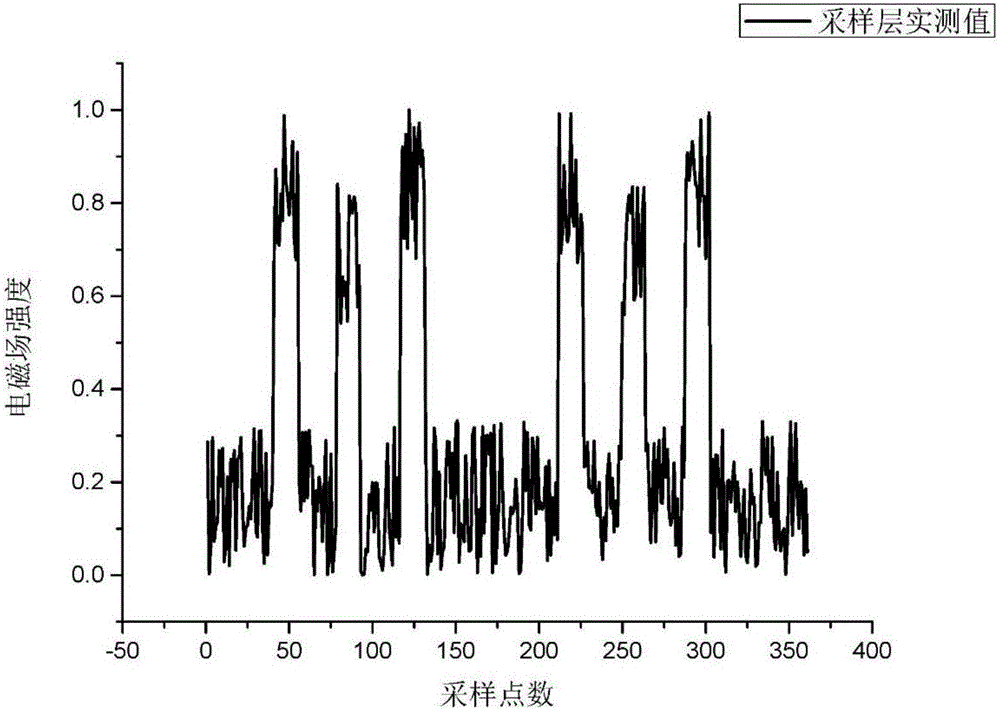
[0113] The electric field and magnetic field probes are used to collect the near-field electric field and magnetic field strength of the PCB circuit at the sampling layer, the mapping matrix T is solved by setting the dipole array, and the dipole moment model matrix is ​​solved by using the regularization algorithm. Different mapping matrices are obtained by changing different observation layers, and then the field intensity distribution on the observation layer is calculated. The relative error is calculated by calculating the numerical value and the simulated numerical value. The relative errors generated by the traditional calculation method and the calculation method of the present invention on different observation layers are shown in Table 1.

[0114] The relative errors produced by the traditional calculation method and the calculation method of the present invention on different observation layers in the embodiment of Table 1

[0115]

[0116] According to the data ...


PUM


Abstract

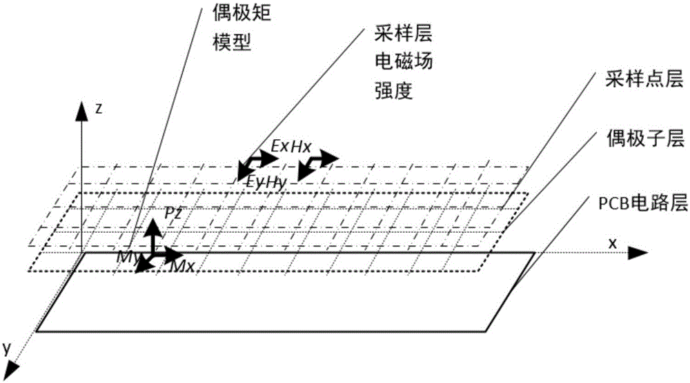
The invention provides a method using a dipole moment model to inverse a PCB circuit electromagnetic field. The method is characterized in that the method comprises the steps that 1 an electromagnetic field probe is used to test near-field electromagnetic field intensity data; 2 a dipole array is set; 3 a mapping matrix T between a sampling point and the dipole array is calculated; 4 a dipole moment matrix X (alpha) is calculated; 5 the tangential electromagnetic field component of the dipole moment matrix X (alpha) on an observation plane at any height above a PCB circuit is calculated; and 6 the tangential electromagnetic field component acquired in step 5 is substituted into formulas (32) and (33) for calculation to solve a normal electromagnetic field component on the plane in step 5. The method has the advantages that voltage and current distribution of the PCB circuit can be well reflected by the matrix; the electromagnetic field radiation can be accurately calculated; the test cost of electromagnetic field distribution is reduced; a powerful basis is provided for the link of system-level electromagnetic compatibility design index quantification verification; the PCB circuit electromagnetic field inversion is realized; and near-field coupling and far-field radiation characteristics of the PCB circuit are acquired.

Description

【Technical field】 [0001] The present invention relates to a method for inversion of electromagnetic field distribution, specifically, equivalent reconstruction of a PCB circuit with unknown physical characteristics using a dipole moment model, and a method for reversing the near-field coupling and far-field radiation of the electromagnetic field of a PCB circuit. way. 【Background technique】 [0002] With the rapid development of electrical engineering, electronic science and technology, computer technology, control theory and control engineering and other technologies, PCB circuits occupy an indispensable position in the application of various industries. The operating frequency band of PCB circuits is continuously expanding, and the integration and complexity are getting higher and higher. Any trace in the PCB circuit may become a source of radiated electromagnetic fields. The coupling between different PCB circuit radiations is the cause of system-level electromagnetic fie...

Claims


Application Information

Patent Timeline
Patent Type & Authority Applications(China)
IPC IPC(8): G01R29/08
CPCG01R29/0892
Inventor 阎照文刘伟王健伟苏东林
Owner BEIHANG UNIV
Learn More