Exclusive OR gate and negation circuit based on local DNA hairpin displacement reaction
A chain displacement reaction and negation circuit technology, which is applied in CAD circuit design, electrical digital data processing, special data processing applications, etc., can solve the problems of slow molecular diffusion and collision of wrong molecules, and achieve fast construction speed and good performance , the effect of improving efficiency
- Summary
- Abstract
- Description
- Claims
- Application Information
AI Technical Summary
Problems solved by technology
Method used
Image
Examples
Embodiment 1
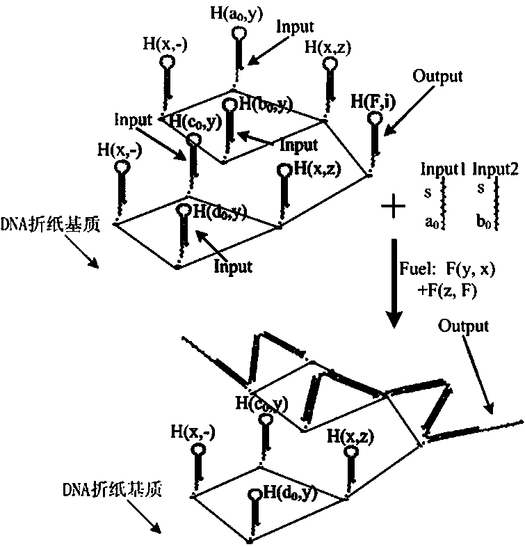
[0030] Such as figure 2As shown, the XOR gate based on the local DNA hairpin strand displacement reaction provided by the present invention is constructed by dual-track logic, including single-stranded DNA input, fuel hairpin and DNA hairpin fixed on the origami substrate;
[0031] The single-stranded DNA input has four: 0 >, 0 >, 0 >, 0 >
[0032] There are two kinds of DNA fuel cards: [s*]{x^> (that is, F(y, x) in the figure), [s*]{F^> (that is, in F(z, F);
[0033] There are seven types of DNA hairpins fixed on the origami substrate: {tether() a 0 ^*}[s]{y^> (that is, H in the figure (a 0 , y), {tether() x^*}[s]{blank^> (that is, H(x, -) in the figure, {tether() b 0 ^*}[s]{y^> (that is, H in the figure (b 0 , y), {tether() x^*}[s]{z^> (that is, H(x, z) in the figure, {tether() c 0 ^*}[s]{y^> (that is, H in the figure (c 0 , y), {tether() d 0 ^*}[s]{y^> (that is, H(d in the figure 0 , y), {tether() F^*}[s]{i^> (that is, H(F, i) in the figure, where tether() means t...
Embodiment 2
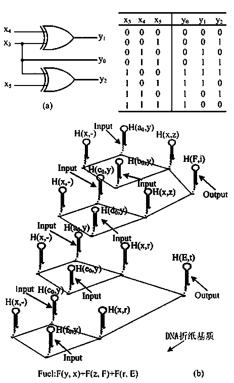
[0289] Such as image 3 As shown, the negation circuit constructed based on the local DNA hairpin displacement reaction XOR gate described in Example 1 belongs to a three-bit binary input negation circuit, which is composed of two parallel XOR gates;
[0290] In this circuit: input x 3 Represents the sign bit of the input binary number, it only has two logic states of "0" and "1", and "0" means that the input binary number is positive, "1" means that the input binary number is negative; input x 4 and x 5 Represent the high and low bits of the binary input value respectively, and also only have two logic states of "0" and "1"; output y 1 and y 2 Respectively represent the high and low bits of the binary output value, and also only have two logic states of "0" and "1";
[0291] The truth table for this negation circuit is as follows:
[0292] .
[0293] It can be seen from the truth table of the negation circuit that when the sign bit x of the binary number is input 3 W...
PUM
 Abstract
Description
Claims
Application Information


