Three-dimensional LED epitaxial structure and preparation method thereof

An epitaxial structure, three-dimensional technology, applied in electrical components, nanotechnology, circuits, etc., can solve the problems of difficult multi-color light emission and high cost of LED epitaxial structure preparation, achieve low process cost, improve electron-hole recombination probability, ratio The effect of large surface area

Inactive Publication Date: 2016-09-07
TAIYUAN UNIV OF TECH
View PDF10 Cites 14 Cited by
  • Summary
  • Abstract
  • Description
  • Claims
  • Application Information

AI Technical Summary

Problems solved by technology

[0006] For this reason, what the present invention aims to solve is the problem that the existing LED epitaxial structure has high preparation cost, and it is difficult to realize multi-color light emission and white light emission.

Method used


Image

  • Three-dimensional LED epitaxial structure and preparation method thereof

Examples


Embodiment

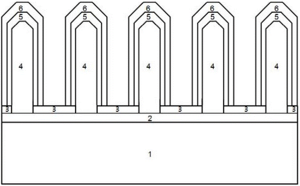
[0038] This embodiment provides a three-dimensional LED epitaxial structure, such as figure 1 As shown, it includes a substrate 1 and porous SiN stacked on the substrate 1 x layer 3; also includes the SiN x The n-type GaN nanorod array 4 in the layer pores is sequentially laminated with a multi-quantum well layer 5 and a p-type GaN layer 6 coated on each surface of the GaN nanorod array 4 .

[0039] The three-dimensional core-shell structure formed by the GaN nanorod array 4 and the multi-quantum well layer 5 and the P-type GaN layer 6 on each outer surface thereof has a large specific surface area. Compared with thin-film materials, more photons can be generated at the same current density, which improves the internal quantum efficiency of the LED epitaxial structure.

[0040] Porous SiN x Layer 3 can not only serve as a growth template for GaN nanorod array 4, but also effectively reduce the dislocation density of the structure and the continued growth of dislocations, th...


PUM

PropertyMeasurementUnit
thicknessaaaaaaaaaa
pore sizeaaaaaaaaaa
heightaaaaaaaaaa

Abstract

The invention relates to the field of a semiconductor, and discloses an LED epitaxial structure. The LED epitaxial structure comprises a substrate and porous SiNx layers laminated on the substrate, and further comprises n-type GaN nano rod arrays formed in apertures of the SiNx layers, multi-quantum well layers which are successively laminated and wrap each surface of the GaN nano rod arrays, and a P-type GaN layer. The GaN nano rod arrays, the multi-quantum well layer wrapping each surface of the GaN nano rod arrays, and the P-type GaN layer form a three-dimensional core shell structure, the specific surface area is large, compared to a thin film material, more photons can be generated under the same current density, and the internal quantum efficiency of the LED epitaxial structure is improved. At the same time, a patterned substrate is unnecessary for growth of the GaN nano rod arrays, and the technical cost is low. The preparation method of the three-dimensional LED epitaxial structure is simple, is easy to implement and low in technical cost and can effectively guarantee the product yield.

Description

technical field [0001] The invention relates to the technical field of semiconductors, in particular to a three-dimensional LED epitaxial structure and a preparation method thereof. Background technique [0002] As a new type of energy-saving light source, GaN-based LED is expected to bring light to as many as 1.5 billion people in the world. However, if it wants to completely replace ordinary lighting and truly enter thousands of households, it needs to further reduce costs, improve luminous intensity and luminous intensity. efficiency. All of these need to be based on the research and development of new high-performance GaN-based LED epitaxial structures, so it is of great significance to carry out research on GaN-based new LED epitaxial structures. [0003] In recent years, GaN-based LEDs have fully realized the industrialization process, but so far, most of the industrialized LED epitaxial structures are based on two-dimensional GaN thin films, and with the increasing d...

Claims


Application Information

Patent Timeline
Patent Type & Authority Applications(China)
IPC IPC(8): H01L33/02H01L33/06H01L33/18H01L33/00B82Y30/00B82Y40/00
CPCH01L33/06B82Y30/00B82Y40/00H01L33/007H01L33/025H01L33/18
Inventor 贾伟赵晨许并社李天保余春燕樊腾仝广运
Owner TAIYUAN UNIV OF TECH
Why Eureka
Try Eureka