
Light splitting chip and preparation method thereof

A chip and spectroscopic technology, applied in the directions of light guides, optics, optical components, etc., can solve the problems of large volume, large cumulative error, and reduced yield of spectrometers, and achieve the effect of simplifying the optical path structure, reducing the volume, and improving the yield.

Pending Publication Date: 2016-09-21
苏州厚朴传感科技有限公司
View PDF7 Cites 3 Cited by
  • Summary
  • Abstract
  • Description
  • Claims
  • Application Information

AI Technical Summary

Problems solved by technology

At present, when making a spectrometer, the spectral light splitting function is mainly realized through a grating, but when the light is split through a grating, the spectrometer is large in size and takes a long time to scan, so it is difficult to achieve true miniaturization
The traditional integrated filter needs to be coated separately for each channel, and each coating needs a specific mask to complete. If there are 64 channels, at least 64 photolithography operations are required. The process is very cumbersome. If the size requirements are high If it is, the cumulative error may be very large, and the yield rate will be reduced; in addition, the size of the traditional integrated filter is large

Method used


Image

  • Light splitting chip and preparation method thereof
  • Light splitting chip and preparation method thereof
  • Light splitting chip and preparation method thereof

Examples


Embodiment 1

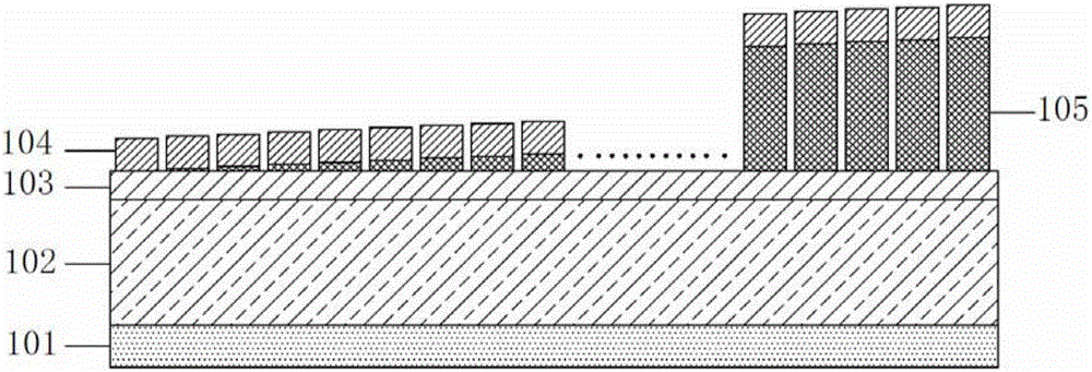
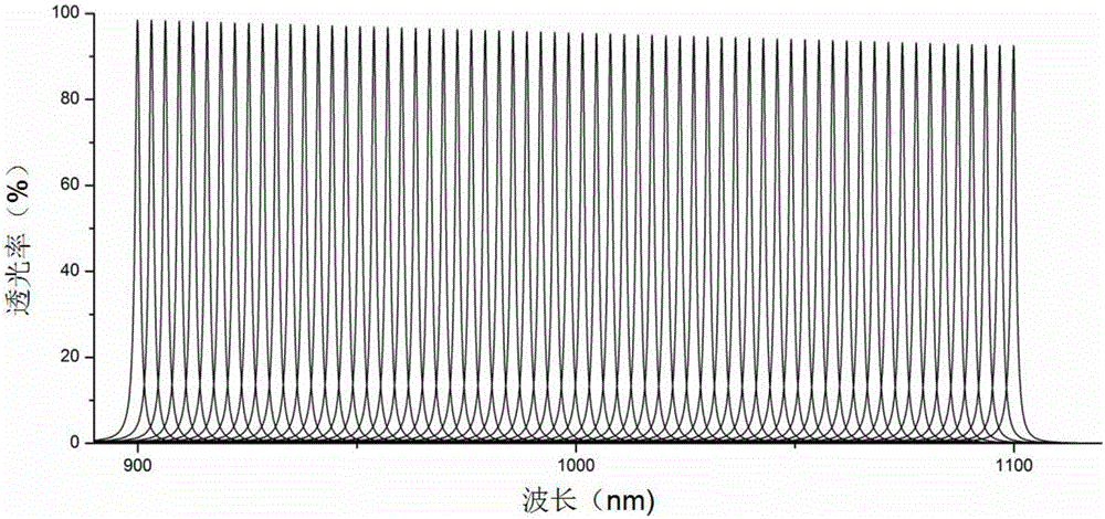
[0062] A spectroscopic chip with a working wavelength of 900-1100nm and a total of 64 channels, numbered 0-63 channels respectively, with a bandwidth of 3.1±1nm and a center wavelength accuracy of ±1nm. The central wavelength increases gradually from channel 0 to channel 63. The width of each channel is in the range of 0.01-2mm, adjacent channels are separated by black chrome, and the width of the chrome line is in the range of 0.001-1mm.

[0063] The specific manufacturing steps of the spectroscopic chip are as follows:

[0064]1. Photoetching channels and alignment marks on the sapphire substrate; wherein the photolithography includes the following steps:

[0065] a) Pretreatment: spin coating photoresist on the clean substrate 102, and bake at 80°C-100°C for more than 10 minutes;

[0066] b) Exposure: place the pretreated substrate under the mask for ultraviolet exposure;

[0067] c) Development and post-baking: the exposed substrate is developed with a developer, the ph...

Embodiment 2

[0083] A spectroscopic chip with a working wavelength of 1100-1400nm and a total of 64 channels, numbered 0-63, with a bandwidth of 4.5±1nm and a center wavelength accuracy of ±1nm. The central wavelength increases gradually from channel 0 to channel 63. The width range of each channel is 0.01-2mm, adjacent channels are separated by black chrome, and the width range of chromium line is 0.001-1mm.

[0084] The specific manufacturing steps of the spectroscopic chip:

[0085] On the sapphire substrate, the steps of photoetching channels and alignment marks, plating the first reflective film, plating the second reflective film and plating the truncation peak film system are the same as in Embodiment 1;

[0086] Wherein, the structure of the first reflection film is: λ=1200nm, H-Nb 2 o 5 , L-SiO 2 , HL H L H L H 3L.

[0087] The film structure of the second reflective film is: λ=1200nm, H-Nb 2 o 5 , L-SiO 2 , HL H L H L H 2L.

[0088] The manufacturing steps of the interme...

Embodiment 3

[0097] A spectroscopic chip with a working wavelength of 1400-1700nm and a total of 64 channels, numbered 0-63, with a bandwidth of 4.5±1nm and a center wavelength accuracy of ±1nm. The central wavelength increases gradually from channel 0 to channel 63. The width of each channel is in the range of 0.01-2mm, adjacent channels are separated by black chrome, and the width of the chrome line is in the range of 0.001-1mm.

[0098] The specific manufacturing steps of the spectroscopic chip:

[0099] On the sapphire substrate, the steps of photoetching channels and alignment marks, plating the first reflective film, plating the second reflective film and plating the truncation peak film system are the same as in Embodiment 1;

[0100] Wherein, the structure of the first reflection film is: λ=1400nm, H-Nb 2 o 5 , L-SiO 2 , HL H L H L H 3L.

[0101] The film structure of the second reflective film is: λ=1400nm, H-Nb 2 o 5 , L-SiO 2 , HL H L H L H 2L.

[0102] The steps of pla...


PUM

PropertyMeasurementUnit
Widthaaaaaaaaaa
Bandwidthaaaaaaaaaa
Widthaaaaaaaaaa

Abstract

The invention discloses a light splitting chip. Sapphire or quartz is taken as a substrate, one side of the substrate is provided with a secondary peak cutting-off film system, the other side of the substrate is provided with a first reflective film, the first reflective film is provided with a plurality of channels, and adjacent channels are separated by black chromium. Simultaneously disclosed is a manufacturing method of the chip. The method comprises the following steps: 1, photoeching the channels and aligning marks on the substrate; 2, coating the first reflective film on the substrate; 3, coating an interface layer; 4, coating a second reflective film; and 5, coating the secondary peak cutting-off film system on the back surface of the substrate. According to the invention, the work wave band of the light splitting chip ranges from 900nm to 2500nm, the dimension can also be adjusted according to actual needs, integration and household application are quite convenient, and the performance of the light splitting chip is far better than the performance of spectrum resolution of conventional similar-type miniaturized spectrometers at home and abroad; genuine miniaturization is realized; and the reliability, the stability and the optical efficiency of an instrument can be improved.

Description

technical field [0001] The invention discloses a light-splitting chip, in particular to a light-splitting chip whose working wave band can be designed according to requirements and a preparation method thereof. Background technique [0002] Near-infrared spectroscopy plays a very important role in the fields of chemical industry, food safety, and health. It mainly uses spectrometers to identify and analyze components, and the requirements for the portability and working speed of spectrometers are getting higher and higher. At present, when making a spectrometer, the spectral light splitting function is mainly realized through a grating, but when the light is split through a grating, the spectrometer has a large volume and a long scanning time, and it is difficult to achieve true miniaturization. The traditional integrated filter needs to be coated separately for each channel, and each coating requires a specific mask to complete. If there are 64 channels, at least 64 photoli...

Claims


Application Information

Patent Timeline
IPC IPC(8): G02B6/125
CPCG02B6/125
Inventor 周东平
Owner 苏州厚朴传感科技有限公司
Learn More