Nanosecond solid-state laser modulation system and bonded wafer separating method

A laser modulation and wafer technology, which is applied in semiconductor/solid-state device manufacturing, laser welding equipment, manufacturing tools, etc., can solve the problems of wasting chemical reagents, affecting yield, and long pre-soaking time, so as to overcome a large number of chemical agents, Solve the effect of long process time and high maintenance cost

Inactive Publication Date: 2016-09-28
NAT CENT FOR ADVANCED PACKAGING
View PDF3 Cites 7 Cited by
  • Summary
  • Abstract
  • Description
  • Claims
  • Application Information

AI Technical Summary

Problems solved by technology

[0004] Temporary bonding technology solves the problem of thin wafer holding and fragmentation during the process, but due to many unstable factors during wafer separation, there is also a great risk of fragmentation during wafer separation
At present, the dielectric treatment methods for wafer separation include heat treatment and Zonebond, etc., but there are certain defects.

Method used


Image

  • Nanosecond solid-state laser modulation system and bonded wafer separating method
  • Nanosecond solid-state laser modulation system and bonded wafer separating method
  • Nanosecond solid-state laser modulation system and bonded wafer separating method

Examples


Embodiment Construction

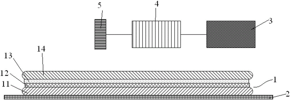
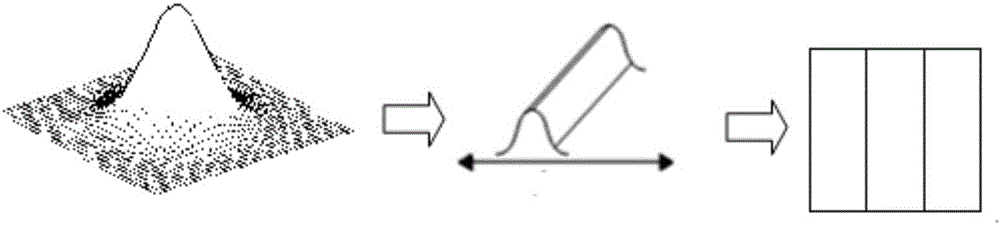
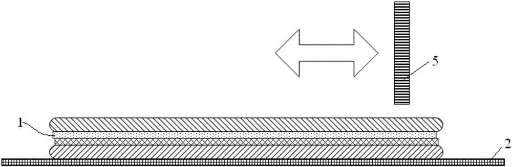
[0029] In order to make the above objects, features and advantages of the present invention more comprehensible, the specific implementation manners of the present invention will be further described below in conjunction with specific drawings.

[0030] In the following description, a lot of specific details are set forth in order to fully understand the present invention, but the present invention can also be implemented in other ways that are different from those described here, and those skilled in the art can do so without departing from the connotation of the present invention. By analogy, the present invention is not limited by the specific examples disclosed below.

[0031] Secondly, the present invention is described in detail in combination with schematic diagrams. When describing the embodiments of the present invention in detail, for the convenience of explanation, the cross-sectional view showing the device structure will not be partially enlarged according to the g...


PUM

PropertyMeasurementUnit
Lengthaaaaaaaaaa
Widthaaaaaaaaaa

Abstract

The invention relates to a nanosecond solid-state laser modulation system and a bonded wafer separating method. The method is characterized by comprising the following steps: (1) placing bonded wafers on a bearing platform; (2) emitting, by a laser generator, Gaussian laser beams, and modulating the Gaussian laser beams via a beam shaping mirror to generate square light spots; focusing the laser beams of the square light spots to penetrate through a glass slide and arrive at a release layer, ashing the releaser layer, and ensuring a bonding layer not damaged; (3) adjusting the relative positions of the laser generator and the bearing platform, so that the moved positions of the square light spots irradiated onto the bonded wafers are ashed, and the light spots after and before moving are partially superposed; sequentially moving the light spots to realize laser irradiation of the whole surface of the bonded wafers; and (4) after laser irradiation and ashing in the above steps, taking the glass slide down. According to the method, the release layer in the temporary bond is ashed by laser, so that batch production can be realized, yield loss is eliminated, and the output efficiency is greatly improved at the same time.

Description

technical field [0001] The invention relates to a process and system for wafer processing, in particular to a nanosecond solid-state laser modulation system and a method for separating bonded wafers, belonging to the technical field of microelectronic packaging. Background technique [0002] With the development of semiconductor technology, electronic devices are getting smaller and smaller, more and more integrated, more and more functions are included, and the overall performance of devices is getting stronger and stronger. Therefore, the production of thin device wafers and thin chips The processing has become a trend in the mass production of ultra-thin products, but because of its instability, temporary bonding and debonding processes have been introduced on this basis. [0003] Temporary bonding and debonding has the following advantages: First, the carrier wafer provides mechanical support and protection for the thin device wafer, so that the backside process can be p...

Claims


Application Information

Patent Timeline
IPC IPC(8): H01L21/683B23K26/50B23K26/073B23K26/08
CPCH01L21/6835B23K26/0732B23K26/0884B23K26/50H01L2221/68318H01L2221/68386
Inventor 姜峰林挺宇李昭强
Owner NAT CENT FOR ADVANCED PACKAGING
Why Eureka
Try Eureka