
Secondary dry etching method based on nanoimprint grating and epitaxial wafer and laser

A technology of nanoimprinting and dry etching, which is applied to the structure of optical resonant cavities, etc., can solve problems such as the large influence of grating etching morphology, threshold current, optical power influence, and difficulty in obtaining grating morphology. Achieve the effect of excellent grating shape, small emission spectral bandwidth and good depth

Active Publication Date: 2019-09-24
INST OF SEMICONDUCTORS - CHINESE ACAD OF SCI
View PDF3 Cites 0 Cited by
  • Summary
  • Abstract
  • Description
  • Claims
  • Application Information

AI Technical Summary

Problems solved by technology

Chlorine-based gas system is easy to generate non-volatile InCl x Reaction product, not conducive to selective etching
The hydrocarbon group generates volatile etching products, which can precisely control the etching depth, but during the etching process, a large amount of polymer will be deposited on the surface of the sample to hinder the further etching, and the chamber will The pressure and ICP power parameters also have a great influence on the etching morphology of the grating
The problem in the current grating etching process is that it is difficult to obtain a smooth and clean grating morphology, and the polymer deposited on the grating surface is not easy to remove, so many defects are introduced, which have a significant impact on the threshold current and optical power

Method used


Image

  • Secondary dry etching method based on nanoimprint grating and epitaxial wafer and laser
  • Secondary dry etching method based on nanoimprint grating and epitaxial wafer and laser
  • Secondary dry etching method based on nanoimprint grating and epitaxial wafer and laser

Examples


Embodiment 1

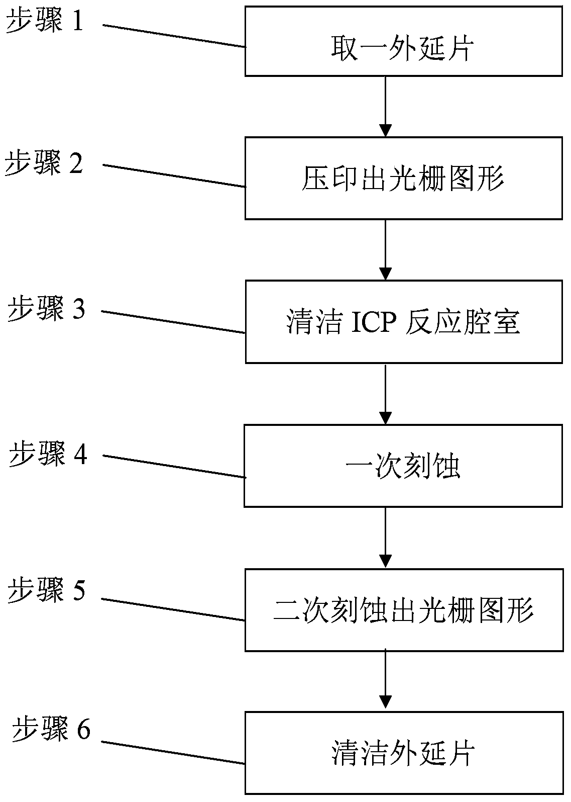
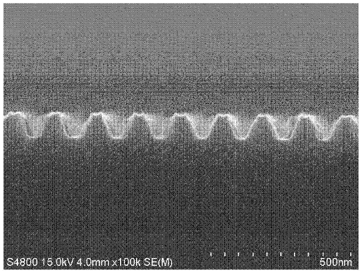
[0030] The secondary dry etching method based on the nanoimprint grating of the present invention, such as figure 1 shown, including the following steps:

[0031] Step 1: Take an epitaxial wafer that has completed one epitaxy, the material of the grating layer is GaInP, and the thickness is about 200nm.

[0032] Step 2: transferring the nanometer pattern on the imprint template to the photoresist coated on the surface of the epitaxial wafer to produce a grating pattern.

[0033] Step 3: Clean the inductively coupled plasma (ICP) reaction chamber to ensure that the chamber is clean and free from contamination. use 2 and SF 6 Mixed gas treatment for 3 minutes, and then O 2 Treatment for 3 minutes is mainly to remove residual organic polymer contamination in the ICP reaction chamber. The cleaning procedure uses 100W of RF power and 1500W of inductively coupled power.

[0034] Step 4: Send the epitaxial wafer with the imprinted grating pattern into the ICP reaction chamber f...

Embodiment 2

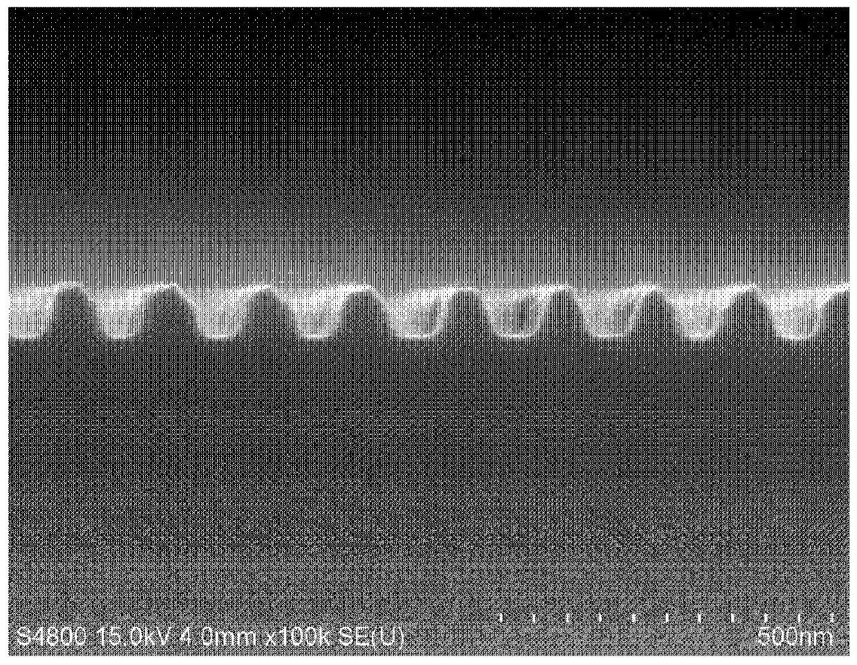
[0045] The secondary dry etching method based on the nanoimprint grating of the present invention, such as figure 1 shown, including the following steps:

[0046] Step 1: Take an epitaxial wafer that has completed one epitaxy, the material of the grating layer is GaInP, and the thickness is about 200nm.

[0047] Step 2: transferring the nanometer pattern on the imprint template to the photoresist coated on the surface of the epitaxial wafer to produce a grating pattern.

[0048] Step 3: Clean the inductively coupled plasma (ICP) reaction chamber to ensure that the chamber is clean and free from contamination. use 2 and SF 6 Mixed gas treatment for 3 minutes, and then O 2 Treatment for 3 minutes is mainly to remove residual organic polymer contamination in the ICP reaction chamber. The cleaning procedure uses 100W of RF power and 1500W of inductively coupled power.

[0049] Step 4: Send the epitaxial wafer with the imprinted grating pattern into the ICP reaction chamber f...


PUM


Abstract

The invention relates to a secondary dry etching method based on a nanoimprint grating, and an epitaxial wafer and a laser. The method comprises steps: through an ultraviolet nanoimprint technology, a grating pattern is imprinted on a photoresist coating the surface of the epitaxial wafer; the well-imprinted epitaxial wafer is fed into a reaction chamber of an inductively coupled plasma (ICP) device for primary etching, wherein the reaction gas is CH4 / H2 / Ar; and the epitaxial wafer with the primary etching completed is fed to the reaction chamber for secondary etching, wherein the reaction gas is CH4 / H2 / Ar. As the secondary dry etching method is adopted, that is, continuous two times of dry etching are carried out on the GaInP grating, an excellent grating topography can be obtained through adjusting and optimizing parameters such as the etched gas flow ratio, the chamber pressure and the etching time.

Description

technical field [0001] The invention belongs to the technical field of semiconductor lasers, relates to a secondary dry etching process, and more specifically relates to a secondary dry etching method based on nanoimprinted gratings and an epitaxial wafer and a laser produced therefrom. Background technique [0002] Distributed feedback lasers (DFB) add Bragg gratings inside the laser to realize optical feedback. Due to the selective effect of the gratings, the output spectral linewidth is much narrower than that of ordinary lasers, and it can stabilize single-mode oscillation. The side-mode suppression ratio and power characteristics of a DFB laser are closely related to the coupling coefficient of the grating, and the coupling coefficient of the grating is determined by factors such as the shape, filling factor, and depth of the grating. Therefore, the characteristics of the grating directly affect the performance of the DFB laser. Therefore, grating preparation is a cruc...

Claims


Application Information

Patent Timeline
Patent Type & Authority Patents(China)
IPC IPC(8): H01S5/12
Inventor 王海丽赵懿昊张奇王文知仲莉刘素平马骁宇
Owner INST OF SEMICONDUCTORS - CHINESE ACAD OF SCI
Learn More