A cmos integrated circuit terahertz source applied in the field of terahertz skin imaging

A skin imaging and integrated circuit technology, applied in the field of terahertz skin imaging, can solve the problems of low surface mobility and low quality factor of passive devices, achieve high conversion gain frequency doubling, wide locking range, and overcome process errors.

Active Publication Date: 2019-04-05
FUDAN UNIV
View PDF4 Cites 0 Cited by
  • Summary
  • Abstract
  • Description
  • Claims
  • Application Information

AI Technical Summary

Problems solved by technology

First, we must study the design of CMOS transistors. CMOS technology has inherent defects when designing terahertz circuits: First, the use of strip polysilicon gates causes high gate resistance, especially in single finger / multi-finger (single finger) / multi-finger ( multi finger) device structure; second, due to the substrate loss characteristics of CMOS at high frequencies, the quality factor of passive devices is very low, usually lower than 10; third, the surface caused by doping scattering Mobility is low, necessitating a targeted physical layout optimization study

Method used


Image

  • A cmos integrated circuit terahertz source applied in the field of terahertz skin imaging
  • A cmos integrated circuit terahertz source applied in the field of terahertz skin imaging
  • A cmos integrated circuit terahertz source applied in the field of terahertz skin imaging

Examples


Embodiment Construction

[0015] The CMOS integrated circuit terahertz source of the present invention applied in the field of terahertz skin imaging will be described in detail below with reference to the accompanying drawings.

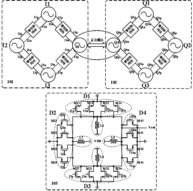
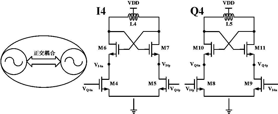
[0016] The circuit structure of the present invention is as attached figure 1 As shown, it is divided into three modules 101, 102 and 103, of which two modules 101 and 102 are 8 cross-coupled oscillator circuits, module 101 is composed of 4 cross-coupled oscillators I1, I2, I3 and I4, and I1 There are zero phase shift network connections between I2, I2 and I3, I3 and I4, I4 and I1 respectively; module 102 is composed of 4 cross-coupled oscillators Q1, Q2, Q3 and Q4, and Q1 and Q2, Q2 and Q3 , Q3 and Q4, Q4 and Q1 are respectively connected by a zero-phase-shift network; I4 and Q4 are connected through quadrature coupling.

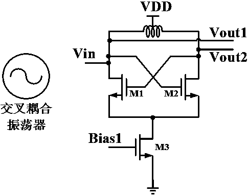
[0017] Among them, the internal structures of I1, I2, I3 and Q1, Q2, Q3 are exactly the same, such as figure 2 As shown, the drains of the NMOS transis...


PUM


Abstract

The invention belongs to the technical field of terahertz CMOS (Complementary Metal Oxide Semiconductors) bio-imaging, in particular to a CMOS integrated circuit terahertz source applied to the terahertz skin imaging field. A novel quadruplicated-frequency injection locking structure is adopted to realize a wide locking range and high conversion gain frequency doubling. A circuit comprises eight cross-coupled oscillators and four frequency multipliers; orthogonal inputs of double-push injection geminate transistors are coupled in a capacitance alternating current way; settings of a grid bias voltage are adjustable; and a largest conversion gain and a widest locking range can be achieved by adjustment of the bias of the double-push injection geminate transistors. When a capacitive load is driven, a locking range close to 60 percent between 300GHz and 400GHz can be realized by an injection locking frequency multiplier; the highest conversion gain can be up to 7dB; the overall power consumption does not exceed 18mW; and the influences of process errors and temperature drift on locking range change, central frequency fluctuation and low output swing are avoided completely.

Description

technical field [0001] The invention belongs to the technical field of terahertz skin imaging, and in particular relates to a CMOS integrated circuit terahertz source. Background technique [0002] With the development of terahertz technology, terahertz-detection medicine (terahertz-LabMed) is currently receiving great attention. Terahertz wave imaging technology has more unique and more applicable physical characteristics, and the photon energy is low, so it will not be harmful to living things. Molecules, biological cells and tissues produce harmful ionization, the radiation dose is almost zero, and the damage to the human body is very small. It is especially suitable for biopsy of biological tissues and provides a new and reliable technical method for human skin imaging research. [0003] Thanks to the reduction of device size and the further development of technology, CMOS integrated circuits have also entered the millimeter wave and even terahertz frequency bands, makin...

Claims


Application Information

Patent Timeline
Patent Type & Authority Patents(China)
IPC IPC(8): H03B5/12H03B19/14A61B5/00
CPCA61B5/00H03B5/1206H03B19/14
Inventor 任俊彦马顺利魏东陈汧
Owner FUDAN UNIV
Why Eureka
Try Eureka