Method for layout OPC (optical proximity correction)

A technology for layout and layout data, applied in the field of layout OPC processing, can solve problems such as affecting device performance, weakening OPC processing effect, yield loss, etc., to achieve the effect of improving fitting degree, increasing layout processing time, and improving processing capacity

Active Publication Date: 2016-11-09
SHANGHAI HUALI MICROELECTRONICS CORP
View PDF4 Cites 11 Cited by
  • Summary
  • Abstract
  • Description
  • Claims
  • Application Information

AI Technical Summary

Problems solved by technology

[0015] Moreover, the general OPC software will take into account the mask plate and photoresist, the influence of the pattern size on the optical model to obtain the optical model, but it often does not take into account the relationship between the pattern density and light transmittance of the customer when establishing the initial optical processing device. There is a considerable difference in the layout data of different customers, which leads to a fixed optical model and graphics processing menu to deal with the layout of different customers. In this way, when the optical processing device has different processing effects on different layouts, it may cause problems. Weaken the actual processing effect of OPC (Optical Proximity Correction), which will further affect the performance of the device, and even cause certain yield loss and other problems

Method used


Image

  • Method for layout OPC (optical proximity correction)

Examples


Embodiment Construction

[0039] In order to make the content of the present invention clearer and easier to understand, the content of the present invention will be described in detail below in conjunction with specific embodiments and accompanying drawings.

[0040] For all stages of integrated circuits from design to manufacturing, the idea of ​​using EDA software is generally used to realize the product. Once the design plan is determined, subsequent tape-out is required to verify the various functions of the design. The verification process includes silicon wafer manufacturing and integration. Circuit processing, packaging, testing and assembly to produce the final product.

[0041] The general process of using EDA software to aid design in integrated circuit design generally includes the following steps:

[0042] System design: EDA software can be used to describe the functions that the designer wants to achieve.

[0043] Logic design and function verification: Designers can use EDA software to ...


PUM


Abstract

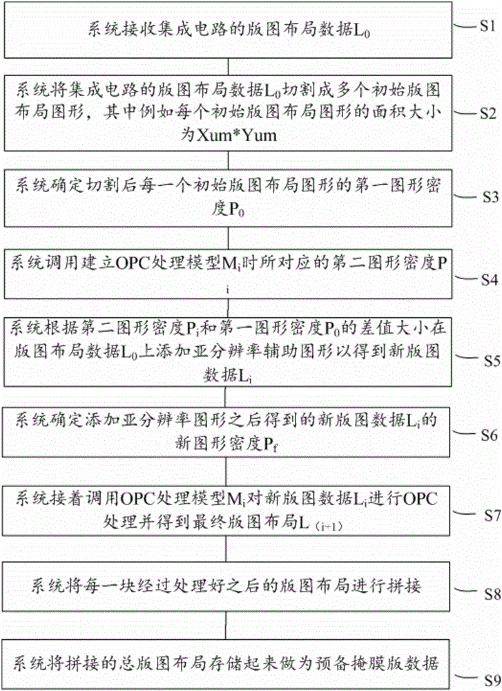
The invention provides a method for layout OPC (optical proximity correction). The method comprises the following steps of enabling a system to receive the layout data of an integrated circuit; enabling the system to divide the layout data of the integrated circuit into a plurality of initial layout graphs; enabling the system to determine a first graph density of each initial layout graph after cutting; enabling the system to call a second graph density when an OPC module is established; enabling the system to add a sub-resolution auxiliary graph onto the layout data according to the difference of first graph density and second graph density, so as to obtain new layout data; enabling the system to determine the new graph density of the new layout data after the sub-resolution graph is added; enabling the system to call the OPC module to perform OPC on the new layout data, and finally obtaining the final layout; enabling the system to splice the layout after OPC; enabling the system to store the whole spliced layout, and use as standby masking layout data.

Description

technical field [0001] The present invention relates to the field of semiconductor manufacturing, and more specifically, the present invention relates to a method for performing layout OPC (Optical Proximity Correction, optical proximity correction) processing. Background technique [0002] At present, large-scale integrated circuits are generally manufactured using photolithography systems. The lithography system is mainly divided into four systems: illumination system, mask, projection system and silicon wafer. The light emitted by the light source is focused by the condenser and then incident on the mask, and the opening part of the mask is light-transmitting; after passing through the mask, the light is incident on the silicon wafer coated with photoresist through the projection system, so that the mask pattern is copied on the wafer . [0003] The rapid development of computational optics makes large-scale integrated circuit technology a step forward. [0004] The pr...

Claims


Application Information

Patent Timeline
Patent Type & Authority Applications(China)
IPC IPC(8): G03F1/36G03F7/20
Inventor 孟鸿林魏芳何大权
Owner SHANGHAI HUALI MICROELECTRONICS CORP
Why Eureka
Try Eureka