
P-channel schottky gate silicon carbide electrostatic induction thyristor and manufacturing method thereof

A technology of Schottky gate and electrostatic induction, which is applied in the direction of thyristor, semiconductor/solid-state device manufacturing, circuit, etc., can solve the problems of increasing the complexity of the driving circuit, limited application value, increasing the driving power, etc., and achieves the reduction of gate switching characteristics , reduce impedance, reduce the effect of process complexity

Pending Publication Date: 2016-11-09
CHANGAN UNIV
View PDF3 Cites 3 Cited by
  • Summary
  • Abstract
  • Description
  • Claims
  • Application Information

AI Technical Summary

Problems solved by technology

[0007] Although the first solution does not increase the difficulty of the process, it needs to change the gate from voltage drive to current drive, which will not only increase the drive power and increase the complexity of the drive circuit; at the same time, because the gate injection can only modulate the low-doped region of the channel conductivity, so the application value of this scheme is limited

Method used


Image

  • P-channel schottky gate silicon carbide electrostatic induction thyristor and manufacturing method thereof
  • P-channel schottky gate silicon carbide electrostatic induction thyristor and manufacturing method thereof
  • P-channel schottky gate silicon carbide electrostatic induction thyristor and manufacturing method thereof

Examples


Embodiment Construction

[0036] The present invention will be further explained below in conjunction with specific embodiments and accompanying drawings.

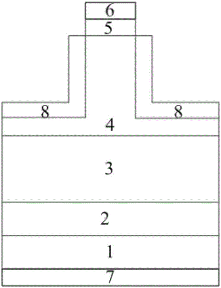
[0037] see figure 1 , the structure of the present invention comprises an N-type SiC substrate 1 and a P-type SiC buffer layer 2 arranged on the top of the N-type SiC substrate, a P-type SiC drift layer 3 is arranged on the P-type SiC buffer layer 2, and the P-type SiC drift layer 3 is provided with a P-type SiC current enhancement layer 4, a P-type SiC ohmic contact layer 5 is provided on the P-type SiC current enhancement layer 4, and a plurality of steps are formed by etching on the P-type current enhancement layer 4 and the P-type SiC ohmic contact layer 5, Grooves are arranged between adjacent steps, Schottky electrodes 8 are arranged on the sides of the steps and at the bottom of the grooves, and a P-type electrode having the same shape as the P-type SiC ohmic contact layer 5 is arranged on the upper part of the P-type SiC ohmic contact layer...


PUM

PropertyMeasurementUnit
thicknessaaaaaaaaaa
thicknessaaaaaaaaaa
thicknessaaaaaaaaaa

Abstract

The invention discloses a P-channel schottky gate silicon carbide electrostatic induction thyristor and a manufacturing method thereof and aims at reducing the on-resistance of a device and improving the power characteristic. According to the technical scheme adopted by the structure, the P-channel schottky gate silicon carbide electrostatic induction thyristor comprises an N-type ohmic contact electrode, an N-type SiC substrate, a P-type SiC buffer layer, a P-type SiC drift layer and a P-type current enhancement layer which are sequentially arranged from bottom to top, wherein a plurality of steps are formed by etching the P-type current enhancement layer; grooves are arranged between the adjacent steps; the top part of each step is provided with a P-type SiC ohmic contact layer; the upper part of each P-type SiC ohmic contact layer is provided with a P-type ohmic contact electrode; the shape of each P-type ohmic contact electrode is the same as that of the corresponding P-type SiC ohmic contact layer; schottky electrodes are arranged in the grooves and are in contact with the side surfaces of the steps and the bottom parts of the grooves; each of the N-type ohmic contact electrode and the P-type ohmic contact electrode comprises an Ni layer and a Pt layer which are sequentially deposited; and each schottky electrode comprises an Ni layer, a Cr layer and an Au layer, or a Ti layer, the Cr layer and the Au layer, or a Pt layer, the Cr layer and the Au layer, which are sequentially deposited.

Description

technical field [0001] The invention relates to the technical field of semiconductor devices and semiconductor technology, in particular to a P-channel Schottky gate silicon carbide electrostatic induction thyristor and a manufacturing method thereof. Background technique [0002] With the rapid development of science and technology, higher and higher requirements are put forward for the performance of power semiconductor devices. Currently used power devices are mainly made of traditional semiconductor materials such as silicon. Due to the limitation of material properties, it is difficult to continuously improve the electrical performance of devices; and devices made of these materials cannot be used in harsh environments such as high temperature and strong radiation. For long-term work, especially in the fields of new energy, automotive electronics, aerospace and other fields, traditional silicon power devices have gradually become incompetent. [0003] Among many new se...

Claims


Application Information

Patent Timeline
Patent Type & Authority Applications(China)
IPC IPC(8): H01L29/74H01L21/332H01L29/06H01L29/47
CPCH01L29/0615H01L29/47H01L29/66363H01L29/74
Inventor 张林张赞朱玮高恬溪
Owner CHANGAN UNIV
Learn More