LVDS (Low Voltage Differential Signaling) interface testing method and system based on FPGA (Field Programmable Gate Array)
An interface testing and interface technology, which is applied in fault hardware testing methods, error detection/correction, detection of faulty computer hardware, etc. Save test time, improve test flexibility and accuracy
- Summary
- Abstract
- Description
- Claims
- Application Information
AI Technical Summary
Problems solved by technology
Method used
Image

Examples
Embodiment Construction
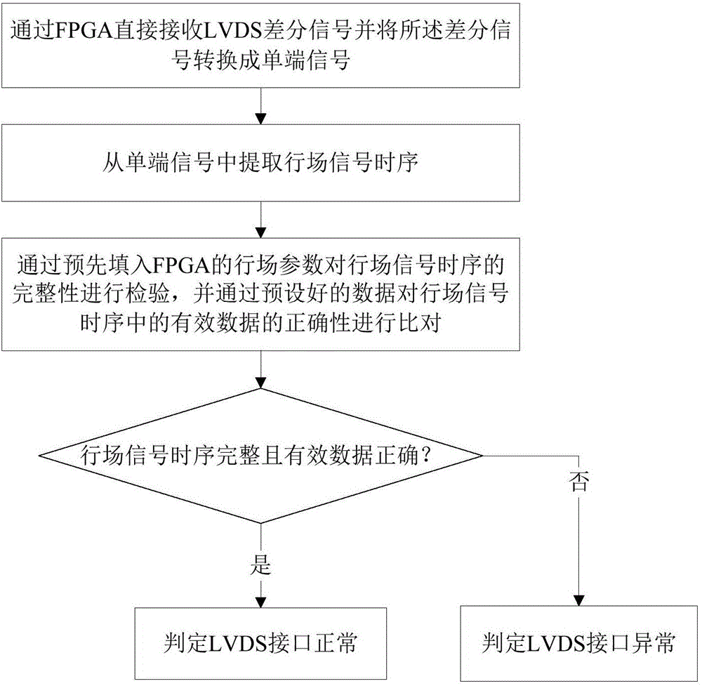
[0026] like figure 1 Shown, a kind of FPGA-based LVDS interface test method comprises the steps:
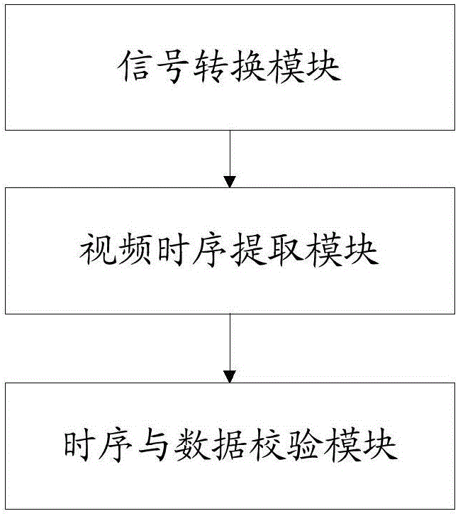
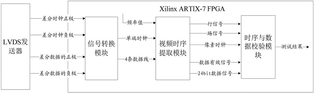
[0027] Step 1, directly receive the LVDS differential signal through the FPGA and convert the differential signal into a single-ended signal; the step 1 is specifically: directly receive the LVDS differential signal through the FPGA, and convert the LVDS differential signal into An identifiable single-ended signal, the single-ended signal includes a single-ended clock and 4 data lines;
[0028] Step 2, extract line field signal timing from single-ended signal; Described step 2 is specifically: use the phase-locked loop inside FPGA according to the frequency value of single-ended clock, and with the input of single-ended clock as phase-locked loop, by lock The phase loop multiplies the frequency and outputs a 7 times frequency clock to sample each bit of data on each data line, and then arranges the timing of the row and field signals. The timing of the row and field signals incl...
PUM
 Abstract
Description
Claims
Application Information
 - Generate Ideas
- Intellectual Property
- Life Sciences
- Materials
- Tech Scout
- Unparalleled Data Quality
- Higher Quality Content
- 60% Fewer Hallucinations
Browse by: Latest US Patents, China's latest patents, Technical Efficacy Thesaurus, Application Domain, Technology Topic, Popular Technical Reports.
© 2025 PatSnap. All rights reserved.Legal|Privacy policy|Modern Slavery Act Transparency Statement|Sitemap|About US| Contact US: help@patsnap.com