A kind of high-quality Aln thin film epitaxially grown on Si substrate and its preparation method
An epitaxial growth, high-quality technology, applied in semiconductor/solid-state device manufacturing, electrical components, circuits, etc., can solve the problems of many influencing factors, long time-consuming, complex growth process, etc., to achieve improved mobility, unique growth process, growth The effect of simple and easy process
- Summary
- Abstract
- Description
- Claims
- Application Information
AI Technical Summary
Problems solved by technology
Method used
Image
Examples
preparation example Construction
[0028] A method for preparing a high-quality AlN film epitaxially grown on a Si substrate, comprising the following steps:
[0029] 1) Select Si substrate;
[0030] Using Si as the substrate, the Si substrate is easy to obtain, cheap, and easy to produce in large sizes, which is conducive to reducing production costs;
[0031] 2) Epitaxial pre-applied Al layer: epitaxially pre-applied Al layer on the Si substrate;
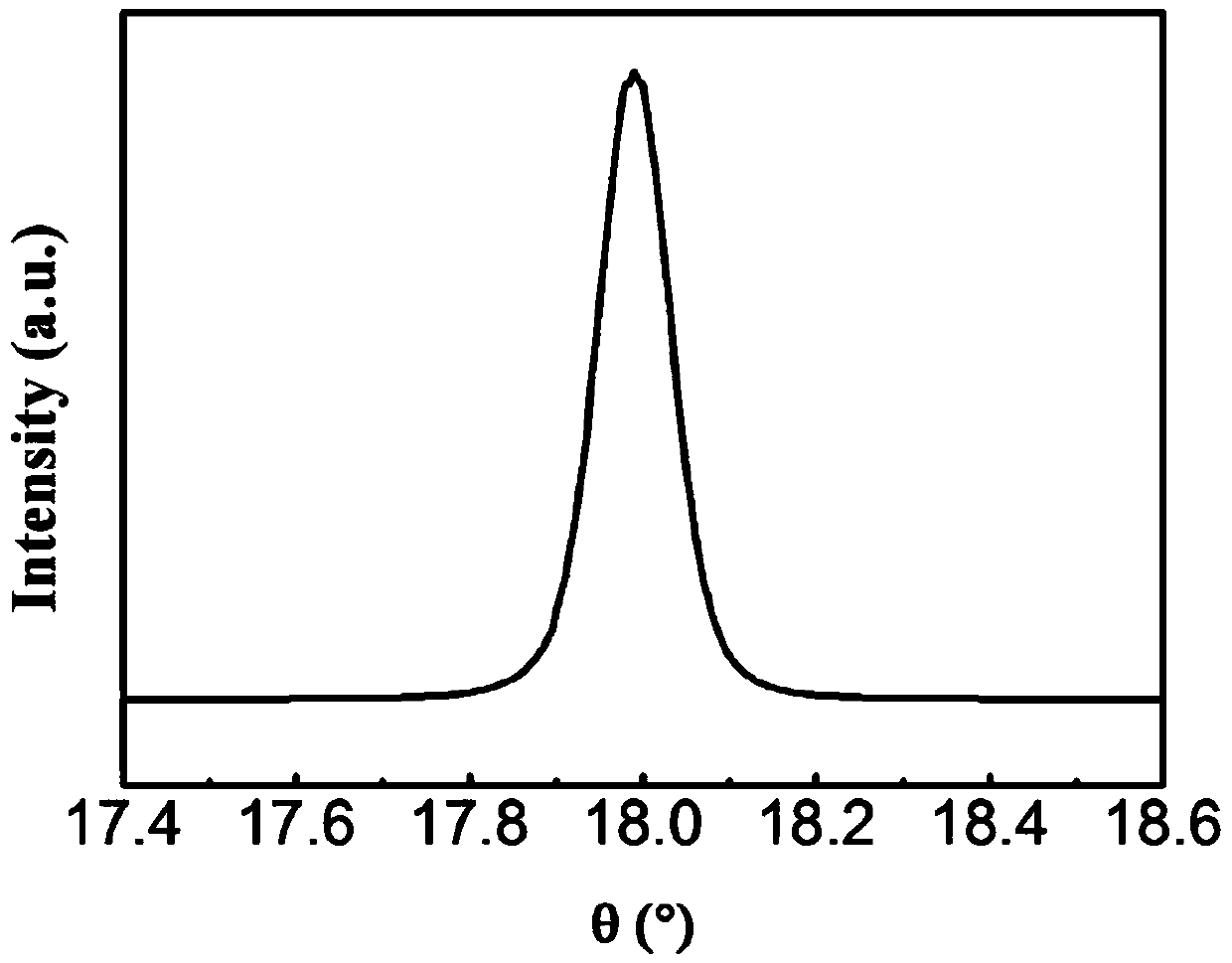
[0032] A layer of Al is pre-laid on the Si substrate to suppress the interface reaction between the Si substrate and the epitaxial layer; then the AlN nucleation layer is grown sequentially to lay the foundation for the further growth of a high-quality AlN film layer, and the obtained The AlN thin film has low dislocation density, small value of half-peak width, and high quality. The method of pre-laying the Al layer includes but is not limited to the use of MOCVD technology;
[0033] 3) Growth of AlN nucleation layer: use NH 3 Carrying out nitriding treatment ...
Embodiment 1
[0037] A method for preparing a high-quality AlN film epitaxially grown on a Si substrate, comprising the following steps:
[0038] 1) Select Si substrate: Si substrate is used, and the epitaxial plane is 0.2-1° away from the (110) direction of the closest-packed plane (111), and the crystal epitaxial orientation relationship is: the (0002) plane of AlN is parallel to that of Si (111) face;
[0039] Surface cleaning and baking of the substrate:
[0040] The specific process of cleaning is: put the Si substrate into H2 mixed with 5% HF 2 SO 4 :H 2 o 2 :H 2 O=3:1:1 ultrasonic cleaning at room temperature in a mixed acid solution for 10-15 seconds to remove the oxide film and organic matter on the surface of the Si substrate, rinse the Si substrate with deionized water, and then ultrasonically wash with deionized water for 1-3 Minutes to remove residual chemical reagents on the surface, and finally blow dry with high-purity dry nitrogen;
[0041] The specific baking proces...
Embodiment 2
[0047] A method for preparing a high-quality AlN film grown on a Si substrate, comprising the following steps:
[0048] 1) Select Si substrate: Si substrate is used, and the epitaxial plane is 0.2-1° away from the (110) direction of the closest-packed plane (111), and the crystal epitaxial orientation relationship is: the (0002) plane of AlN is parallel to that of Si (111) surface;
[0049] The specific process of cleaning is: put the Si substrate into H2 mixed with 5% HF 2 SO 4 :H 2 o 2 :H 2 O=3:1:1 ultrasonic cleaning at room temperature in a mixed acid solution for 10-15 seconds to remove the oxide film and organic matter on the surface of the Si substrate, rinse the Si substrate with deionized water, and then ultrasonically wash with deionized water for 1-3 Minutes to remove residual chemical reagents on the surface, and finally blow dry with high-purity dry nitrogen;
[0050] The specific process of baking is as follows: put the substrate into the MOCVD reaction cha...
PUM
| Property | Measurement | Unit |
|---|---|---|
| thickness | aaaaa | aaaaa |
| thickness | aaaaa | aaaaa |
Abstract
Description
Claims
Application Information
 - R&D
- Intellectual Property
- Life Sciences
- Materials
- Tech Scout
- Unparalleled Data Quality
- Higher Quality Content
- 60% Fewer Hallucinations
Browse by: Latest US Patents, China's latest patents, Technical Efficacy Thesaurus, Application Domain, Technology Topic, Popular Technical Reports.
© 2025 PatSnap. All rights reserved.Legal|Privacy policy|Modern Slavery Act Transparency Statement|Sitemap|About US| Contact US: help@patsnap.com


