Flash memory device forming method

A technology of memory and flash memory, which is applied in the field of formation of flash memory, can solve problems such as the failure of programming crosstalk in split-gate flash memory, and achieve the effect of increasing resistance, reducing grinding loss, and reducing programming crosstalk

Active Publication Date: 2016-11-16
SHANGHAI HUAHONG GRACE SEMICON MFG CORP
View PDF3 Cites 9 Cited by
  • Summary
  • Abstract
  • Description
  • Claims
  • Application Information

AI Technical Summary

Problems solved by technology

[0004] However, the existing split-gate flash memory has a serious problem of programming crosstalk failure

Method used


Image

  • Flash memory device forming method
  • Flash memory device forming method
  • Flash memory device forming method

Examples


Embodiment Construction

[0022] As mentioned in the background art, the split-gate flash memory formed in the prior art has a serious problem of programming crosstalk failure.

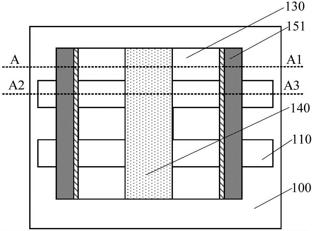
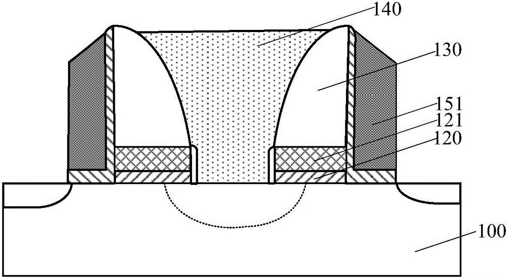
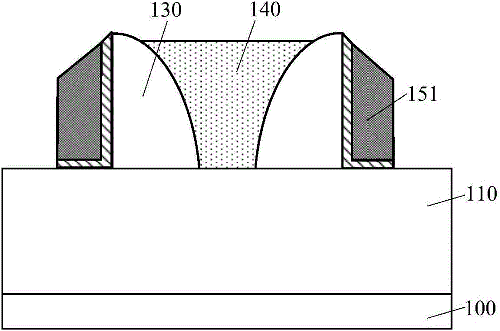
[0023] figure 1 is a schematic diagram of the structure of a flash memory, figure 2 for along figure 1 The schematic diagram obtained by cutting line A-A1 in, image 3 for along figure 1 Schematic obtained by cutting line A2-A3.

[0024] refer to figure 1 , figure 2 and image 3 The method for forming the flash memory includes: providing a semiconductor substrate 100; forming a floating gate oxide layer and a floating gate layer on part of the semiconductor substrate 100, the floating gate layer being located on the floating gate oxide layer; forming an isolation layer in the semiconductor substrate 110, the isolation layer 110 is located on both sides of the floating gate oxide layer and the floating gate layer; forming a separate dielectric layer across the floating gate oxide layer, floating gate layer and isolatio...


PUM


Abstract

A flash memory device forming method is disclosed and comprises the following steps: a semiconductor substrate having word line digit line zones and source line floating gate zones, floating gate oxidation layers and floating gate layers that stretch across the word line digit line zones and the source line floating gate zones are formed on parts of the semiconductor substrate, isolating layers positioned at two sides of the floating gate oxidation layers and the floating gate layers are formed in the semiconductor substrate, dielectric layers covering the word line digit line zones are formed, first openings are arranged between the dielectric layers, first side walls are formed on side walls of the first openings, the floating gate layers and the floating gate oxidation layers positioned at bottom parts of the first openings are removed, and second openings are therefore formed; in the first openings and the second openings, source line films are formed on the first side walls and the dielectric layers, the source line films on the first side walls and the dielectric layers are removed via grinding operation, and an excessive grinding amount in grinding processes can be obtained according to distance between surfaces of top parts of the isolating layers and surfaces of top parts of the floating gate layers; after the dielectric layers, the floating gate layers and the floating gate oxidation layers at the word line digit line zones, word line structures are formed at the word line digit line zones. Via use of the method, a programming crosstalk failure occurrence can be lowered.

Description

technical field [0001] The invention relates to the field of semiconductor manufacturing, in particular to a method for forming a flash memory. Background technique [0002] Flash memory is an important device in integrated circuit products. The main feature of flash memory is that it can keep stored information for a long time without applying voltage. Flash memory has the advantages of high integration, fast access speed and easy erasing, so it is widely used. [0003] Flash memory is classified into two types: stack gate flash memory and split gate flash memory. The stacked gate flash memory has a floating gate and a control gate above the floating gate. The stacked gate flash memory has the problem of over-erasing. Different from the stacked gate flash memory, the split gate flash memory forms a word line as an erasing gate on one side of the floating gate. The split-gate flash memory can effectively avoid the over-erasing effect. In addition, the split-gate flash ...

Claims


Application Information

Patent Timeline
Patent Type & Authority Applications(China)
IPC IPC(8): H01L21/8247
CPCH10B41/00H10B41/40
Inventor 徐涛曹子贵王卉陈宏
Owner SHANGHAI HUAHONG GRACE SEMICON MFG CORP
Why Eureka
Try Eureka