Flexible CIGS film solar cell module inner joint method

A thin-film solar cell, copper indium gallium selenide technology, applied in the field of solar cells, can solve the problems of poor reliability of the preparation process, increased dead area of ​​components, short circuit or leakage of the battery, etc. The effect of improving reliability and production yield

Active Publication Date: 2016-11-16
CHINA ELECTRONIC TECH GRP CORP NO 18 RES INST
View PDF11 Cites 6 Cited by
  • Summary
  • Abstract
  • Description
  • Claims
  • Application Information

AI Technical Summary

Problems solved by technology

[0004] In the publicly available inline method of flexible copper indium gallium selenide thin film solar cell modules, either the process steps are interspersed between the three scribing lines, or the scribing process requires overlaying, which will make accurate positioning difficult and the components will die. The area area increases, the light-receiving area decreases, and the photoelectric conversion efficiency decreases, and the production process steps are cumbersome and time-consuming, and the production efficiency is low
There are still many technical difficulties in using the all-laser method for depth selective etching to complete the three scribe lines, especially the first scribe line that acts as the bottom electrode of the segregation cell. The layer, absorbing layer and back electrode are all removed, exposing the substrate, and the laser scribing will cause melting. The material recrystallized after melting in the channel has good electrical conductivity, and it is very easy to cause the connection of the positive and negative electrodes of the sub-battery, causing a short circuit of the battery. or electric leakage, the reliability of the component preparation process is poor, and the production yield is low

Method used


Image

  • Flexible CIGS film solar cell module inner joint method
  • Flexible CIGS film solar cell module inner joint method
  • Flexible CIGS film solar cell module inner joint method

Examples


Embodiment Construction

[0028] In order to further understand the invention content, characteristics and effects of the present invention, the following examples are given, and detailed descriptions are as follows in conjunction with the accompanying drawings:

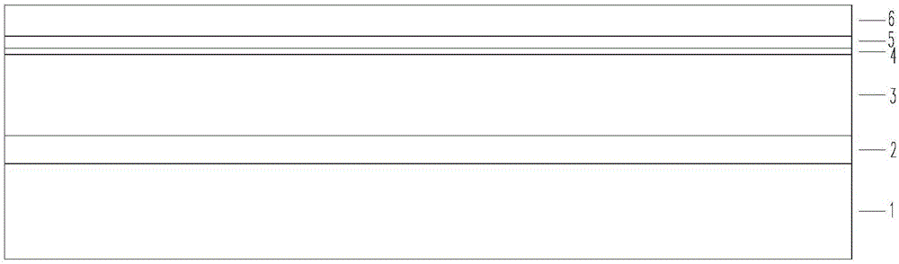
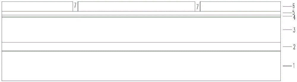
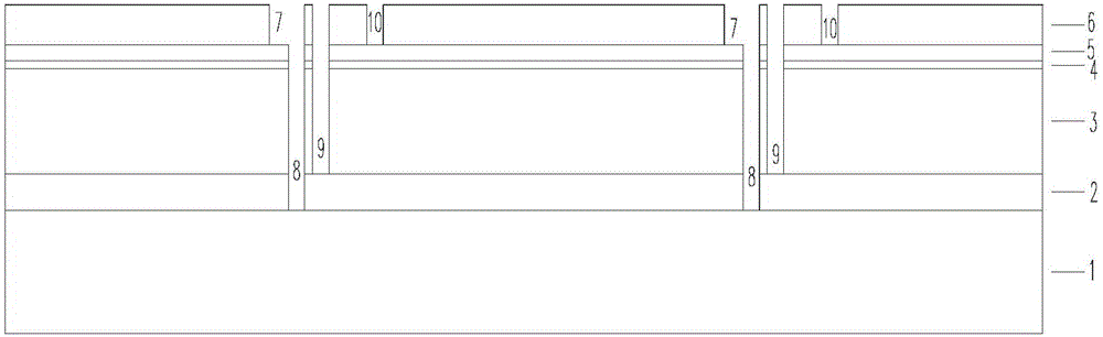
[0029] see Figure 5 , a flexible copper indium gallium selenide thin film solar cell module inline method, the flexible copper indium gallium selenide thin film solar cell sequentially comprises: a substrate 1, a back electrode layer 2, an absorption layer 3, a buffer layer 4, High resistance layer 5, transparent conductive layer 6;

[0030] see Figure 1 to Figure 5 , including the following steps:

[0031] Step 101, using laser etching to etch at least one pretreatment channel 7 from top to bottom on the transparent conductive layer 6; preferably, in this embodiment, there are two parallel pretreatment channels 7; The bottom surface of the processing channel 7 is the upper surface of the high resistance layer 5;

[0032] Step 102: Etch...


PUM


Abstract

The invention discloses a flexible CIGS (Cu(In,Ga)Se2) film solar cell module inner joint method, comprising the steps of: step 1, employing a laser etching method to etch at least one pretreatment channel on a transparent conducting layer, the bottom of the pretreatment channel being the upper surface of a high resistance layer; step 2, employing a laser etching method to respectively etch a first channel, a second channel, and a third channel on one side of each pretreatment channel, wherein one side of the first channel is in communication with the pretreatment channel, the bottom of the first channel is the upper surface of a substrate, the second channel is located between the first channel and a third channel, the bottom of the second channel is the upper surface of a back electrode layer, and the bottom of the third channel is located between the upper surface of the high resistance layer and the upper surface of the back electrode layer; step 3, pouring an insulation material in the first channel and the pretreatment channel and performing solidification; step 4, employing a silk-screen printing method to print silver paste and performing solidification; and step 5, solidifying an electrode material.

Description

technical field [0001] The invention relates to the technical field of solar cells, in particular to a method for inlining flexible copper indium gallium selenium thin film solar cell components. Background technique [0002] Flexible Copper Indium Gallium Selenium Cu(In,Ga)Se 2 (referred to as CIGS) thin-film solar cells have the characteristics of high mass specific power, rollable, flexible unfolding, and portability, and have a wide range of applications. [0003] In practical applications, the output voltage of solar cells is usually greater than the open-circuit voltage of a single cell. Separate a large-area thin-film solar cell into several independent sub-cells and connect them in series to obtain a higher output voltage. [0004] In the publicly available inline method of flexible copper indium gallium selenide thin film solar cell modules, either the process steps are interspersed between the three scribing lines, or the scribing process requires overlaying, whic...

Claims


Application Information

Patent Timeline
Patent Type & Authority Applications(China)
IPC IPC(8): H01L31/0463H01L31/0465
CPCY02E10/50H01L31/0463H01L31/0465
Inventor 闫礼乔在祥冯洋刘洋张超冯金晖
Owner CHINA ELECTRONIC TECH GRP CORP NO 18 RES INST
Why Eureka
Try Eureka