A method of manufacturing a high-precision pressure sensor based on silicon-silicon bonding

A technology of a pressure sensor and a manufacturing method, applied in the field of silicon micromechanical sensors, can solve the problems of difficult implementation of process means, deformation of thin diaphragms, sensitive resistance lithography accuracy and precise control of appearance dimensions, etc. The effect of small static pressure error and reduction of processing difficulty

Active Publication Date: 2018-11-06
SHENYANG ACAD OF INSTR SCI
View PDF9 Cites 0 Cited by
  • Summary
  • Abstract
  • Description
  • Claims
  • Application Information

AI Technical Summary

Problems solved by technology

For gauge pressure and differential pressure sensors that are more widely used, it is necessary to bond the bottom silicon with a through hole. The existence of the through hole has brought great restrictions to the implementation of the back-end process after silicon-silicon bonding. Some Conventional techniques are difficult to implement
In addition, sensors based on silicon-silicon bonding usually first thin the top layer of silicon and process it into a stress film area, and then process the piezoresistor. The existence of a vacuum cavity and subsequent processes may cause deformation of the thinner diaphragm, which is sensitive The lithographic accuracy of the resistor and the precise control of the appearance size may have an impact

Method used


Image

  • A method of manufacturing a high-precision pressure sensor based on silicon-silicon bonding
  • A method of manufacturing a high-precision pressure sensor based on silicon-silicon bonding
  • A method of manufacturing a high-precision pressure sensor based on silicon-silicon bonding

Examples


Embodiment 1

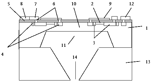
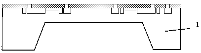
[0057] Such as figure 1 As shown, the pressure sensor of the present invention comprises a sensitive silicon chip layer 1 and a substrate silicon chip layer 13, the back side of the sensitive silicon chip layer 1 is connected with a substrate silicon chip layer 13, and the sensitive silicon chip layer 1 and the substrate silicon chip layer 13 adopt A silicon-silicon bonding process forms a pressure-tight cavity.

[0058] Such as figure 1 with figure 2 As shown, the sensitive silicon layer is based on a single crystal silicon material, a pressure diaphragm 10 is arranged on the surface of the chip, a concave silicon cup 11 is arranged under the pressure diaphragm, and a piezoresistor 2 is arranged on the pressure diaphragm; The varistor 2 is divided into two sections and consists of resistors connected to the P+ connection area 3. The varistor 2 is connected to the lead hole 6 through the P+ connection area 3. A metal lead 7 is arranged above the lead hole 6 of the P+ connec...


PUM


Abstract

The invention discloses a manufacturing method of a high-precision pressure sensor based on silicon-silicon bonding. The high-precision pressure sensor comprises a sensitive silicon wafer layer and a substrate silicon wafer layer and is characterized in that the substrate silicon wafer layer is connected to the back of the sensitive silicon wafer layer, and the sensitive silicon wafer layer and the substrate silicon wafer layer use silicon-silicon bonding process to form a pressure sealing cavity; the substrate silicon wafer layer and the sensitive silicon wafer layer are made of homogenous monocrystalline silicon materials, and the substrate silicon wafer layer is provided with a pressure guide through hole in the center. The manufacturing method has the advantages that the substrate silicon wafer layer and the sensitive silicon wafer layer are made by using the monocrystalline silicon materials as the substrates, the substrate silicon wafer layer and the sensitive silicon wafer layer are connected in an airtight manner through the silicon-silicon bonding process, the pressure sealing cavity of a silicon-silicon homogenous material structure is formed, various influences, caused by the pressure sealing cavity of the silicon-glass heterogeneous material structure of a conventional pressure sensor, on the performance of the sensor due to the feature difference of two different materials are avoided, static pressure errors are reduced effectively, temperature excursion of the sensor is lowered, and the comprehensive precision of the sensor is increased.

Description

technical field [0001] The invention belongs to the technical field of silicon micromechanical sensors, in particular to a method for manufacturing a high-precision pressure sensor based on silicon-silicon bonding using single-crystal silicon materials. Background technique [0002] As a typical representative of the great success of micromachining technology, piezoresistive pressure sensors are widely used in many fields such as industrial control, environmental monitoring and measurement, automotive systems, aerospace, military, and biomedicine. The sensitive chip of the piezoresistive pressure sensor is made of single crystal silicon material, which is made by the fusion technology of microelectronics and micromachining. It has the characteristics of good linearity and easy signal measurement. However, due to the temperature characteristics of the piezoresistive sensor piezoresistor itself and the characteristics of the packaging structure, it is not only sensitive to the...

Claims


Application Information

Patent Timeline
Patent Type & Authority Patents(China)
IPC IPC(8): G01L1/18
CPCG01L1/18
Inventor 李颖张治国郑东明梁峭祝永峰
Owner SHENYANG ACAD OF INSTR SCI
Why Eureka
Try Eureka