

Method of alloying wafer after wiring
An alloying and wafer technology, applied in semiconductor devices, electrical components, circuits, etc., can solve problems such as affecting the stability and size of NMOS capacitor C, unable to repair the quality of gate oxide, and failure of oscillation frequency, and achieve improvement. Product yield, repair quality, and effect of reducing interface state density
- Summary
- Abstract
- Description
- Claims
- Application Information
AI Technical Summary
Problems solved by technology
Method used
Image

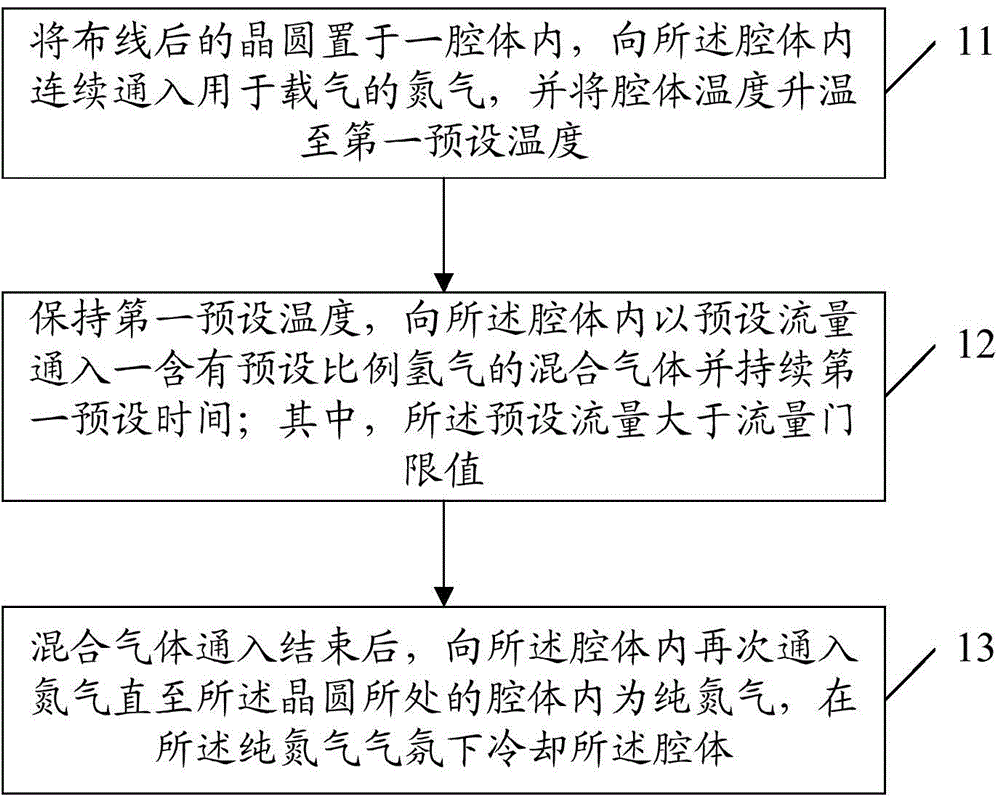
Examples
Embodiment Construction
[0027] In order to make the technical problems, technical solutions and advantages to be solved by the present invention clearer, the following will describe in detail with reference to the drawings and specific embodiments.
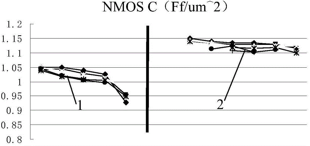
[0028] The present invention aims at the problem of frequency failure of NMOS capacitors caused in the alloying process in the CMOS process technology in the prior art, and provides a method for alloying wafers after wiring. The optimization of the alloy, that is, the increase of the flow rate of the preset ratio of hydrogen in the alloy, will more effectively passivate the Si (silicon) dangling bonds near the interface without damaging the gate oxide structure of the wafer, and greatly reduce the interface state density. , repair the quality of the gate oxide, thereby changing the C-V curve characteristics of the NMOS capacitor, and then achieve the purpose of improving the frequency failure, and at the same time improve the product yield; on the other h...
PUM
 Abstract
Description
Claims
Application Information