Low-pass filter based on TSV (Through-Silicon-Via) technology

A low-pass filter and through-silicon via technology, which is applied in the field of filters, can solve problems such as occupying a large board area, difficulties in filters and couplers, and technology that cannot meet the requirements of integrated circuits, so as to save costs, improve integration, The effect of reducing the occupied area

Active Publication Date: 2016-11-23
西安国创电子股份有限公司
View PDF4 Cites 25 Cited by
  • Summary
  • Abstract
  • Description
  • Claims
  • Application Information

AI Technical Summary

Problems solved by technology

[0002] Today, mobile wireless devices such as smartphones, tablets, and ultrabooks have the advantages of miniaturization, high speed, and multiple functions. Moreover, these devices can also implement different communication standards. In order to solve these challenging requirements, system-in-package and system Advanced packaging technologies such as chip-level chip technology are rapidly developing to integrate communication systems into a small package; however, packaging traditional RF passive components such as filters, couplers, and antennas is quite difficult, mainly due to their bulky size, so the RF passives had to be moved out of the package and designed in PCB circuit board; and mounting these passive components requires a large PCB Board area
[0003] In order to meet the design requirements of the filter, the footprint is small enough or even does not occupy PCB Board area requirements, the initial effort is to find materials with high dielectric constant, high quality factor and low frequency temperature coefficient, and this technology can only reduce the size of the device to the order of centimeters or millimeters, which is already very small, but with the integration of circuits With the continuous improvement of the degree, the technology cannot meet the requirements of the current integrated circuit

Method used


Image

  • Low-pass filter based on TSV (Through-Silicon-Via) technology
  • Low-pass filter based on TSV (Through-Silicon-Via) technology
  • Low-pass filter based on TSV (Through-Silicon-Via) technology

Examples


Embodiment 1

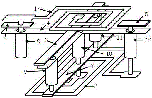
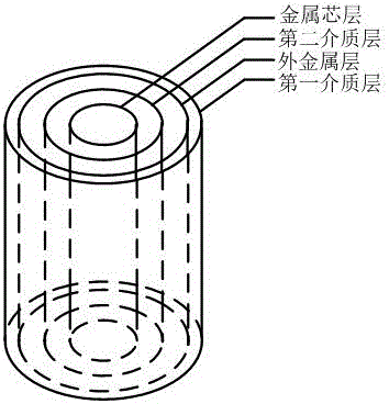
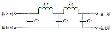
[0021] Such as figure 1 As shown, a schematic structural diagram of a low-pass filter based on the TSV technology of the present invention, a low-pass filter based on the TSV technology, including a spiral inductor unit, a rewiring layer and a TSV component, wherein , the spiral inductor unit is composed of a spiral inductor 1 and a spiral inductor 2 2, the rewiring layer includes an input terminal 3, an output terminal 5, a ground metal 4, an interconnection layer 1 6 and an interconnection layer 2 7, and the TSV component includes Five coaxial TSVs with the same structure, respectively TSV 1 8, TSV 2 9, TSV 3 10, TSV 4 11 and TSV 5 12, coaxial TSVs It includes the first dielectric layer, the outer metal layer, the second dielectric layer and the metal core layer in sequence from outside to inside, such as figure 2 As shown, a schematic diagram of the coaxial TSV structure in a low-pass filter based on TSV technology of the present invention.

[0022] The outer metal laye...

Embodiment 2

[0025] On the basis of Example 1, the spiral inductor 1 and the spiral inductor 2 both include a central end and an end, and the tops of the metal core layers of the TSV 9 , TSV 3 10 and TSV 4 11 pass through the interconnection layer One 6 is connected and connected to the central end of the spiral inductor one 1, the bottom is connected through the interconnection layer two 7 and connected to the central end of the spiral inductor two 2, the top of the metal core layer of the through-silicon via one 8 is connected to the input terminal 3 and the spiral inductor The ends of the first 1 are connected, the top of the metal core layer of the TSV 12 is connected to the output end 5, and the bottom is connected to the end of the spiral inductor 2 2 .

[0026] The second TSV 9 , the third TSV 10 and the fourth TSV 11 are connected in parallel for the purpose of connecting the equivalent capacitance of the TSV in parallel to increase the capacitance value.

Embodiment 3

[0028] On the basis of the above embodiments, the first dielectric layer is preferably one of a silicon dioxide layer, a silicon nitride layer and a silicon oxynitride layer, and is used to electrically isolate the TSV from the surrounding silicon substrate.

[0029] The second dielectric layer is preferably a hafnium dioxide layer with a high dielectric constant, and its function is to realize electrical isolation between the outer metal layer and the metal core layer in the TSV.


PUM


Abstract

The invention relates to a filter, in particular to a low-pass filter based on TSV (Through-Silicon-Via) technology. The low-pass filter based on the TSV technology comprises a spiral inductance unit, a rewiring layer and a TSV component, wherein the spiral inductance unit comprises a spiral inductor I and a spiral inductor II, the rewiring layer comprises an input end, an output end, grounding metal, an interconnecting layer I and an interconnecting layer II, the TSV component comprises five coaxial through silicon vias of a through silicon via I, a through silicon via II, a through silicon via III, a through silicon via IV and a through silicon via V respectively which are the same in structure, and each coaxial through silicon via comprises a first dielectric layer, an outer metal layer, a second dielectric layer and a metal core layer in sequence from outside to inside; according to the invention, the coaxial through silicon vias are adopted to realize vertical capacitors, compared with the common plane structure capacitors, the occupied areas of the capacitors are greatly reduced, and the sizes of the devices are reduced to micron magnitudes, so that the circuit integration can be improved, and further the cost is reduced.

Description

technical field [0001] The invention belongs to filters, in particular to a low-pass filter based on silicon through hole technology. Background technique [0002] Today, mobile wireless devices such as smartphones, tablets, and ultrabooks have the advantages of miniaturization, high speed, and multiple functions. Moreover, these devices can also implement different communication standards. In order to solve these challenging requirements, system-in-package and system Advanced packaging technologies such as chip-level chip technology are rapidly developing to integrate communication systems into a small package; however, packaging traditional RF passive components such as filters, couplers, and antennas is quite difficult, mainly due to their bulky size, so the RF passives had to be moved out of the package and designed in PCB circuit board; and mounting these passive components requires a large PCB board area. [0003] In order to meet the design requirements of the filt...

Claims


Application Information

Patent Timeline
Patent Type & Authority Applications(China)
IPC IPC(8): H01L23/64
CPCH01L23/642
Inventor 王凤娟王刚余宁梅
Owner 西安国创电子股份有限公司
Why Eureka
Try Eureka