Single-crystal silicon-based nano-inverted pyramid-structured back-passivated solar cells

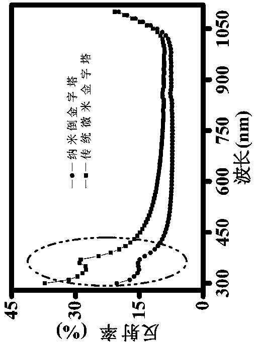
A nano-inverted pyramid and solar cell technology, which is applied in the field of solar cells, can solve the problems of low spectral response of battery devices, low external quantum efficiency of batteries, and general anti-reflection ability, etc., to improve short-wave spectral response, improve photoelectric conversion efficiency, The effect of excellent photoelectric performance

Active Publication Date: 2018-08-21
HUAIHAI INST OF TECH
View PDF7 Cites 0 Cited by
  • Summary
  • Abstract
  • Description
  • Claims
  • Application Information

AI Technical Summary

Problems solved by technology

Its defect is that the spectral response of battery devices in the short-wavelength band (300nm-450nm) and long-wavelength band (900nm-1200nm) is not high, and there is room for further improvement
The main reason is that the anti-reflection ability of the front pyramid structure is average, resulting in low external quantum efficiency in the short-wave band; the surface recombination rate of the aluminum back field on the back is relatively high, resulting in low external quantum efficiency of the battery in the long-wave band

Method used


Image

  • Single-crystal silicon-based nano-inverted pyramid-structured back-passivated solar cells
  • Single-crystal silicon-based nano-inverted pyramid-structured back-passivated solar cells
  • Single-crystal silicon-based nano-inverted pyramid-structured back-passivated solar cells

Examples


Embodiment 1

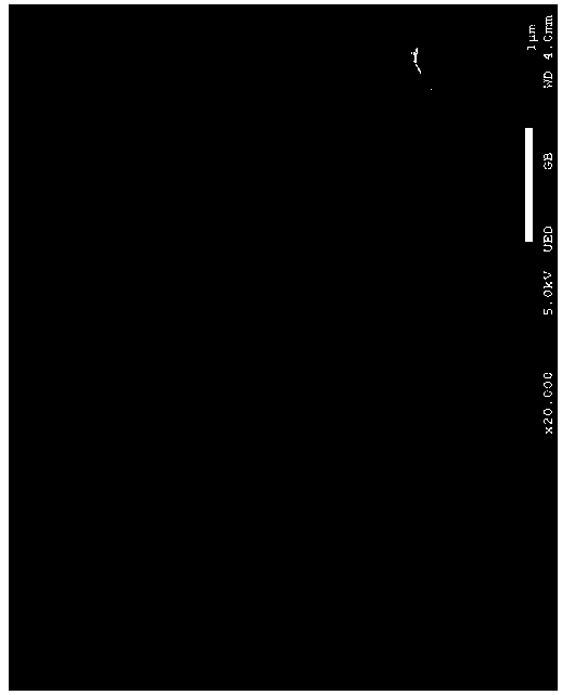
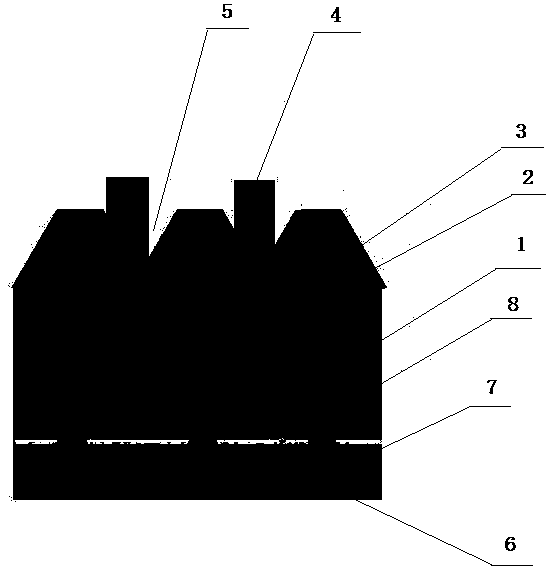
[0033] Embodiment 1, with reference to figure 1 and figure 2 , a monocrystalline silicon-based nano-inverted pyramid structure back passivated solar cell: comprising a mono-crystalline silicon substrate 1, the front surface of the mono-crystalline silicon substrate 1 adopts a nano-inverted pyramid structure emitter 5, and the back surface of the mono-crystalline silicon substrate 1 A back passivation structure is adopted; the silicon nanometer inverted pyramid structure emitter 5 is composed of a silicon nanometer inverted pyramid structure and two passivation dielectric films.

[0034] Wherein, the back passivation structure adopts PECVD-SiO 2 / SiN x stack passivation. The side length of the opening on the silicon nanometer inverted pyramid structure is 700nm-900nm, and the depth is 800nm-1000nm.

[0035] In the two-layer passivation dielectric film: the inner passivation dielectric film is SiO deposited by PECVD 2 Thin film 2, with a thickness of 9nm-11nm; the outer pa...

Embodiment 2

[0037] Embodiment 2, in a kind of monocrystalline silicon-based nano-inverted pyramid structure back passivation solar cell described in embodiment 1:

[0038] The side length of the opening on the silicon nanometer inverted pyramid structure is 800nm, and the depth is 900nm. In the two-layer passivation dielectric film: the inner passivation dielectric film is SiO deposited by PECVD 2 Film 2, with a thickness of 10nm; the outer passivation dielectric film is SiN deposited by PECVD x Thin film 3 has a thickness of 70 nm. The back passivation structure consists of two passivation dielectric films, the inner passivation dielectric film is SiO deposited by PECVD 2 Film 8 with a thickness of 25nm; the outer passivation dielectric film is SiN deposited by PECVD x Thin film 7 has a thickness of 250 nm.

Embodiment 3

[0039] Embodiment 3, a kind of preparation method of monocrystalline silicon-based nano-inverted pyramid structure rear passivation solar cell, its steps are as follows:

[0040] (1) Silicon wafer preparation: use p-type surface-cut, solar-grade Cz silicon wafer as the substrate, and clean the silicon wafer with RCA standard process to obtain a single crystal silicon substrate;

[0041] (2) Preparation of nanoporous silicon: by HF, AgNO 3 、H 2 o 2 In the mixed solution, the nanoporous silicon structure is etched on the front surface of the single crystal silicon substrate by using MACE (metal-assisted chemical etching method), the etching time is 50 seconds to 70 seconds, and then HNO 3 solution to clean the residual silver; in the mixture: the concentration of HF is 1.9M-2.1M, AgNO 3 The concentration is 0.004M-0.006M, H 2 o 2 The concentration is 1.00M-1.10M;

[0042] (3) Preparation of nano-inverted pyramid structure: put the nano-porous silicon wafer into NaOH soluti...


PUM

PropertyMeasurementUnit
thicknessaaaaaaaaaa
thicknessaaaaaaaaaa
thicknessaaaaaaaaaa

Abstract

The invention provides a mono-crystalline-silicon-based back-passivated solar cell with a nano inverted pyramid structure. The mono-crystalline-silicon-based back-passivated solar cell is characterized by comprising a mono-crystalline silicon substrate; the front surface of the mono-crystalline silicon substrate adopts a nano inverted pyramid structure emitting electrode; the back surface of the mono-crystalline silicon substrate adopts a back-passivated structure; the silicon nano inverted pyramid structure emitting electrode is composed of a silicon nano inverted pyramid structure and two layers of passivated dielectric films. The invention further relates to a preparation method of the mono-crystalline-silicon-based back-passivated solar cell with the nano inverted pyramid structure. Spectral responses of the cell on a short-wave band and a long-wave band are optimized, and excellent spectral response of the silicon-based solar cell on a whole wave band (with the wavelength of 300nm to 1100nm) is realized; finally, the efficiency of the solar cell is improved. Meanwhile, excellent photoelectric properties of the front surface (short wave) and the back surface (long wave) are guaranteed.

Description

technical field [0001] The invention relates to a solar cell, in particular to a monocrystalline silicon-based nanometer inverted pyramid structure back passivated solar cell; the invention also relates to a preparation method of the aforementioned solar cell. Background technique [0002] Excellent broadband spectral response is of great and decisive significance for improving the photoelectric conversion efficiency of solar cells. At present, commercially produced large-area crystalline silicon solar cells have shown good spectral response in the mid-band 500nm-800nm. Satisfactory spectral response, mainly because the front side of the cell still has high residual reflection and the back side of the cell comes from the large surface recombination loss of the aluminum back field. In order to further improve the performance of the battery and realize the excellent spectral response of the battery in a wide band, it is necessary to simultaneously optimize the photoelectric p...

Claims


Application Information

Patent Timeline
Patent Type & Authority Patents(China)
IPC IPC(8): H01L31/0224H01L31/0216H01L31/18
CPCH01L31/02168H01L31/022425H01L31/18Y02E10/50Y02P70/50
Inventor 黄增光朱旭东
Owner HUAIHAI INST OF TECH
Why Eureka
Try Eureka