Silicon carbide metal oxide semiconductor field effect transistor and manufacturing method thereof

An oxide semiconductor and field effect transistor technology, which is applied in semiconductor/solid-state device manufacturing, semiconductor devices, electrical components, etc., can solve the problem of increasing circuit overhead, cannot respond well to the temperature of silicon carbide VDMOS devices in the package, and does not have timely performance. It can reduce the layout cost, reduce the cost, and achieve the effect of good compatibility.

Active Publication Date: 2016-12-07
INST OF MICROELECTRONICS CHINESE ACAD OF SCI
View PDF3 Cites 2 Cited by
  • Summary
  • Abstract
  • Description
  • Claims
  • Application Information

AI Technical Summary

Problems solved by technology

[0004] In the process of realizing the present invention, the inventor found that there are at least the following technical problems in the prior art: using peripheral circuits to detect the operating temperature of silicon carbide VDMOS devices increases the overhead of the circuit, and at the same time does not have timeliness; using sensors to detect silicon carbide VDMOS The operating temperature of the device is for the detection of the temperature after packaging, which cannot well reflect the temperature of the silicon carbide VDMOS device in the package.

Method used


Image

  • Silicon carbide metal oxide semiconductor field effect transistor and manufacturing method thereof
  • Silicon carbide metal oxide semiconductor field effect transistor and manufacturing method thereof
  • Silicon carbide metal oxide semiconductor field effect transistor and manufacturing method thereof

Examples


Embodiment Construction

[0030] In order to make the purpose, technical solutions and advantages of the embodiments of the present invention clearer, the technical solutions in the embodiments of the present invention will be clearly and completely described below in conjunction with the drawings in the embodiments of the present invention. Obviously, the described embodiments It is only some embodiments of the present invention, but not all embodiments. Based on the embodiments of the present invention, all other embodiments obtained by persons of ordinary skill in the art without making creative efforts belong to the protection scope of the present invention.

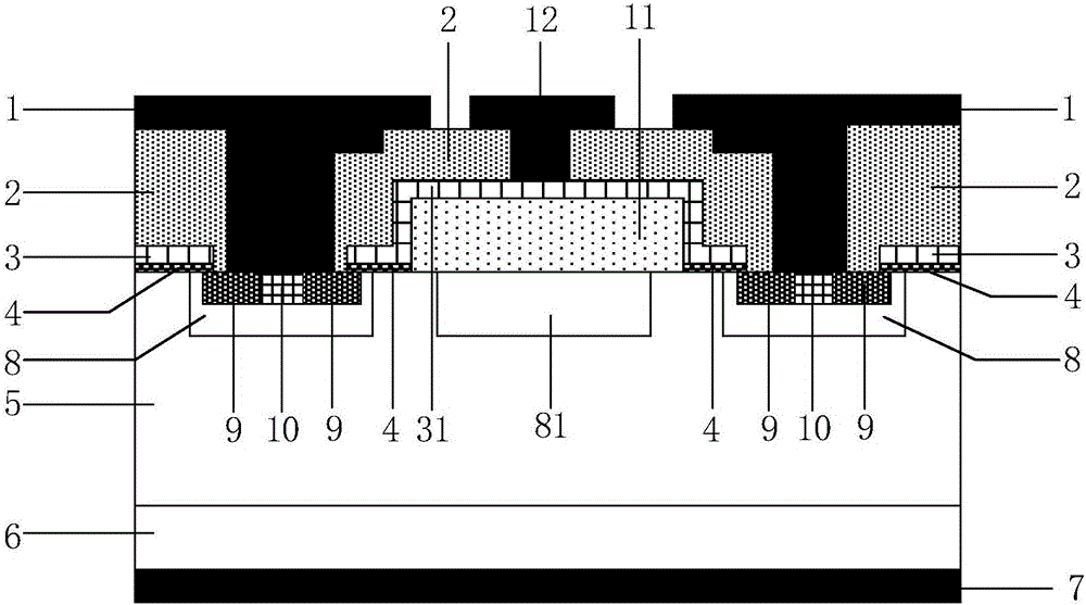
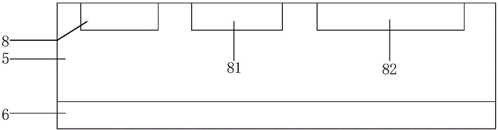
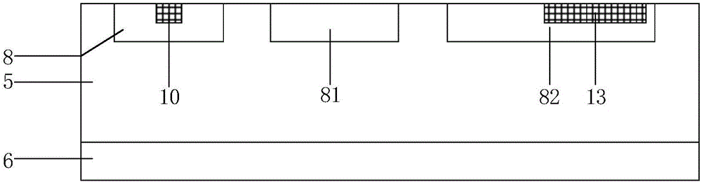
[0031] figure 1 It is a schematic diagram of the structure of a traditional SiC VDMOS device, in figure 1 Among them, 1 is metal source electrode, 2 is interlayer dielectric, 3 is polysilicon gate, 4 is gate dielectric, 5 is silicon carbide N - Drift region, 6 is silicon carbide N + Substrate, 7 is the metal drain electrode, 8 is the first...


PUM


Abstract

The invention provides a silicon carbide metal oxide semiconductor field effect transistor and a manufacturing method thereof. A temperature sensor P+ ion implantation region and a temperature sensor N+ ion implantation region are formed in a third P well region through ion implantation; and the temperature sensor P+ ion implantation region and the temperature sensor N+ ion implantation region form a PN junction diode. Real-time detection of an internal temperature of a silicon carbide device is achieved through integrating a PN junction temperature sensor in a P well of a silicon carbide VDMOS; the silicon carbide metal oxide semiconductor field effect transistor can be applied to temperature detection at a high temperature; the influence of the sensor on reverse withstand voltage of the silicon carbide VDMOS is eliminated; the layout overhead is minimized; and the silicon carbide metal oxide semiconductor field effect transistor has good compatibility with an existing VDMOS manufacturing technology.

Description

technical field [0001] The invention relates to the technical field of semiconductor devices, in particular to a silicon carbide metal oxide semiconductor field effect transistor and a manufacturing method thereof. Background technique [0002] With the characteristics of high critical breakdown electric field, high thermal conductivity, high hot carrier saturation drift speed, and strong radiation resistance, silicon carbide (Silicon Carbide) material greatly expands the energy handling capacity of power devices and meets the requirements of the following A generation of power electronic equipment requires higher power, smaller size and harsher working conditions for power devices, which are gradually being applied to various electronic system fields. [0003] Silicon carbide VDMOS is often used in high-power devices. It works under high-voltage and high-current conditions, and it will generate a lot of heat when it is turned on and off repeatedly. If it is not regulated i...

Claims


Application Information

Patent Timeline
Patent Type & Authority Applications(China)
IPC IPC(8): H01L21/336H01L21/78
CPCH01L29/66712H01L29/7817
Inventor 宋凌云申华军汤益丹邓小川白云郭飞柏思宇
Owner INST OF MICROELECTRONICS CHINESE ACAD OF SCI
Why Eureka
Try Eureka