Semiconductor device

A semiconductor and device technology, applied in the field of semiconductor devices, can solve problems such as device instability

Active Publication Date: 2016-12-14
SICHUAN HONGXINWEI TECH
View PDF12 Cites 0 Cited by
  • Summary
  • Abstract
  • Description
  • Claims
  • Application Information

AI Technical Summary

Problems solved by technology

These effects, individually or cumulatively, will lead to important semiconductor device characteristics, such as breakdown voltage and reverse current, especially under HTRB and / or H3TRB (high humidity-high temperature-high reverse voltage) conditions, the device will not Stablize

Method used


Image

  • Semiconductor device

Examples


Embodiment Construction

[0018] Embodiments of the present invention will be described in detail below with reference to the accompanying drawings.

[0019] An embodiment of the present invention is: n-type nano-silicon particles (doped with phosphorus, concentration 10 18 cm -3 ) mixed with photosensitive polyimide (such as Hitachi-DuPont HD-4100) at a volume concentration of 30%. This was followed by ball milling at 80˚C for 96 hours, sonication for 3 hours, and spin-coating on wafers. Pattern lithography is carried out by using well-known photolithography technology, and then polymerization, metallization and other processes are performed as in the disclosed technology of polymer passivation high-voltage semiconductor devices, and a semiconductor device with a mesa structure or a planar structure is produced.

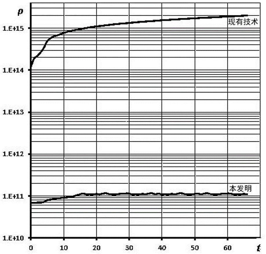
[0020] In a 10 μm film containing nanocomposite material based on the aforementioned Hitachi-DuPont polyimide, we observed that the surface resistance of the glass passivation layer (measu...


PUM


Abstract

In order to reduce the ageing and degeneration of the characteristics of a semiconductor device under high reverse bias and high temperature conditions, a polymer, such as polyimide, is taken as a passivation layer of the semiconductor device. According to the invention, the polymer material and the semiconductor device nanometer grain with distribution grain size of 4-8 debye length are mixed at a volume ratio of 15%-40% and are poured and formed into the passivation layer.

Description

technical field [0001] This invention is commonly used in semiconductor devices, especially in polymer-based surface passivation devices, such as polyimide passivation layers, suitable for high voltage applications. In particular, the invention applies to high reliability devices, especially under high reverse bias stress (HTRB) conditions. Background technique [0002] As we all know, due to the high sensitivity of device parameters to contamination and surface mobile charges near the PN junction, the surface passivation technology of semiconductor devices is one of the main measures to obtain high reliability in demanding applications. Among the various passivation designs and methods, known prior art, technologies based on inorganic and organic materials are widely used. Such as the glass passivation technology announced by US Patent US3212921 published on October 19, 1965 and US Patent US3241010 published on March 23, 1962; The polymer passivation technology announced ...

Claims


Application Information

Patent Timeline
Patent Type & Authority Applications(China)
IPC IPC(8): H01L29/06
CPCH01L29/0615
Inventor 李学良西里奥·艾·珀里亚科夫
Owner SICHUAN HONGXINWEI TECH
Why Eureka
Try Eureka