High consistency resistive random access memory and preparation method thereof

A resistive memory, resistive thin film technology, applied in electrical components and other directions, can solve problems such as fluctuation, instability, and restricting the integration density of resistive memory

Active Publication Date: 2016-12-14
PEKING UNIV
View PDF5 Cites 6 Cited by
  • Summary
  • Abstract
  • Description
  • Claims
  • Application Information

AI Technical Summary

Problems solved by technology

[0004] However, due to the random generation and fusing characteristics of the conductive channel in the resistive memory, it will cause problems with the consistency of the device, that is, the parameters of the corresponding resistive change, such as operating voltage, high-resistance state and low-resistance state resistance. Will fluctuate between different devices and different switching processes of the same device
This unstable characteristic restricts the improvement of the integration density of resistive memory, and also increases the difficulty of peripheral circuit design. Therefore, reducing device volatility and improving device consistency are of great significance for the industrial application of resistive memory.

Method used


Image

  • High consistency resistive random access memory and preparation method thereof
  • High consistency resistive random access memory and preparation method thereof
  • High consistency resistive random access memory and preparation method thereof

Examples


specific Embodiment

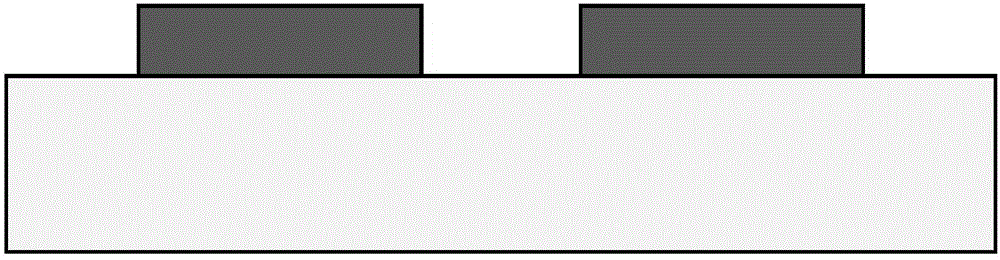
[0030] 1) Select the substrate material used, which can be selected according to the application; for example, choose Si substrate;

[0031] 2) The lower electrode pattern is defined by photolithography, and the metal lower electrode is deposited by PVD or evaporation. The material of the lower electrode can be Pt, TaN, Ir, etc., such as figure 2 shown;

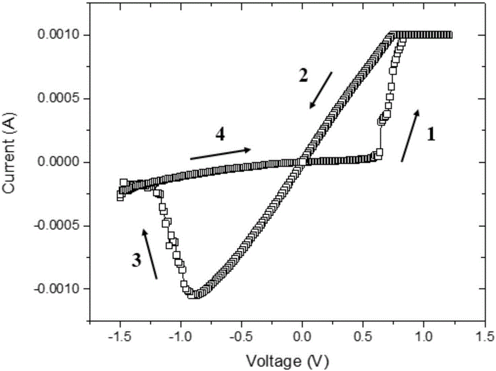
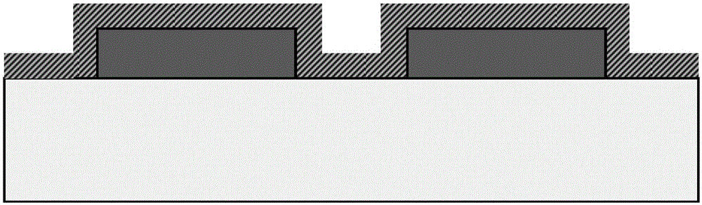
[0032] 3) Prepare a layer of resistive thin film material by PVD reactive sputtering method: the specific material can be TaOx, HfOx, etc., with a thickness between 30nm-100nm, such as image 3 shown;

[0033] 4) The local doping area is defined by photolithography, that is, the symmetrical central area of ​​the upper and lower electrode intersection (stack) area of ​​the device. The implantation area is half of the device area, that is, the area of ​​the upper electrode, and Au is implanted by ion implantation. + ions, such as Figure 4 shown;

[0034] 5) The lower electrode lead-out hole is defined by photolithography,...


PUM


Abstract

The invention provides a high consistency resistive random access memory and a preparation method thereof, and belongs to the technical field of CMOS very large scale integration. The resistive random access memory comprises a substrate and a lower electrode-resistance variation film-upper electrode structure which is located on the substrate; the lower electrode is located on the substrate; the resistance variation film is located between the upper and lower electrodes; the resistance variation film is locally doped with metals; and the doped region is 50% to 10% of a device working area. A conducting channel of the resistive random access memory is more easily fused at a locally doped area, thus random generation and fusion of the conducting channel are limited in the locally doped area, the randomness of the conducting channel is effectively reduced, and the consistency of the resistive random access memory is improved.

Description

technical field [0001] The invention belongs to the technical field of non-volatile memory (Non-volatile Memory) in semiconductor (semiconductor) and CMOS ultra-large-scale integration (ULSI), in particular to a resistive random access memory (resistive random access memory) with high consistency Device structure design and fabrication method. Background technique [0002] Since the invention of the transistor, the development of semiconductor and integrated circuit technology has promoted the progress of the entire information industry and even technology. For nearly half a century, following the prediction of Moore's Law, the integration level of memory devices based on CMOS technology has grown rapidly at a rate of doubling every 18 months. However, as the feature size continues to shrink, especially after entering the nano-scale node, the size reduction of the current mainstream memories will reach the limit. Traditional non-volatile memory is facing more and more chal...

Claims


Application Information

Patent Timeline
Patent Type & Authority Applications(China)
IPC IPC(8): H01L45/00
CPCH10N70/881H10N70/011H10N70/043
Inventor 蔡一茂王宗巍黄如康健方亦陈喻志臻杨雪
Owner PEKING UNIV
Why Eureka
Try Eureka