Method for Batch Inspection of Semiconductor Devices Using Graphene Probes

A batch detection and semiconductor technology, which is applied in the direction of single semiconductor device testing, instrumentation, measuring electricity, etc., can solve the problems of inapplicability, achieve the effect of reducing detection cost, improving sensitivity and accuracy, and improving the level of automation and adaptability

Active Publication Date: 2019-04-16
YANTAI TAIXIN ELECTRONICS TECH CO LTD
View PDF6 Cites 0 Cited by
  • Summary
  • Abstract
  • Description
  • Claims
  • Application Information

AI Technical Summary

Problems solved by technology

However, this scheme is not applicable in some occasions that require high precision

Method used


Image

  • Method for Batch Inspection of Semiconductor Devices Using Graphene Probes
  • Method for Batch Inspection of Semiconductor Devices Using Graphene Probes
  • Method for Batch Inspection of Semiconductor Devices Using Graphene Probes

Examples


Embodiment Construction

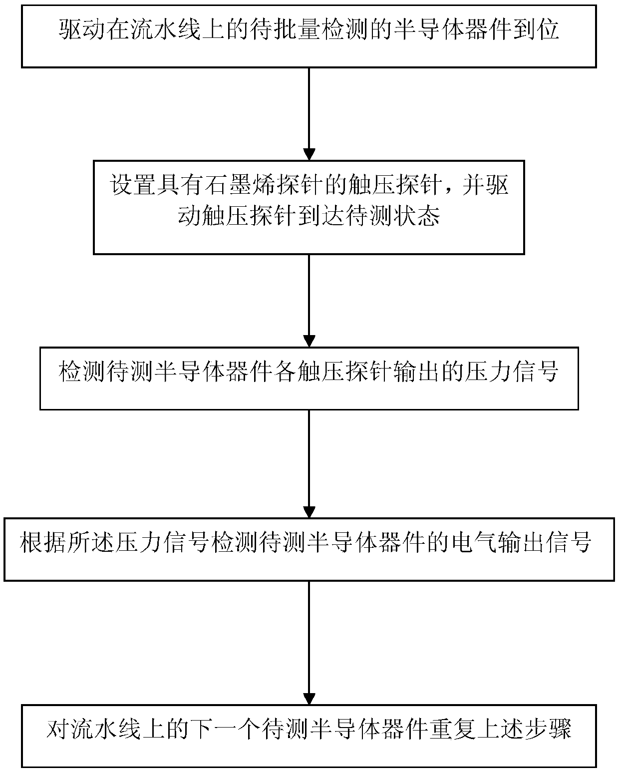
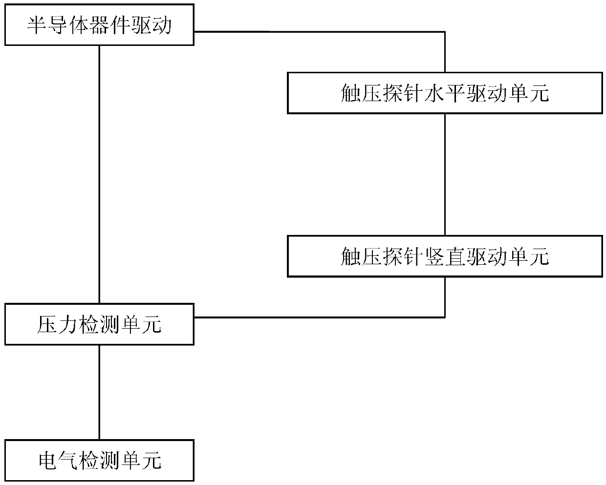
[0047] like figure 2 As shown, the detection system of the present invention based on having graphene probes for batch detection of semiconductor devices includes: semiconductor device drive unit, touch pressure probe horizontal drive unit, touch pressure probe vertical drive unit, electrical detection unit and pressure detection unit, the semiconductor device drive unit, the touch probe horizontal drive unit and the touch probe vertical drive unit are connected in series by the drive signal line and driven sequentially, that is, the driving completion signal of the semiconductor device drive unit is used as The drive start signal of the touch pressure probe horizontal drive unit, the drive completion signal of the touch pressure probe horizontal drive unit is used as the drive start signal of the touch pressure probe vertical drive unit, and the pressure detection unit The driving completion signal of the vertical driving unit of the contact pressure probe is used as the dri...


PUM


Abstract

In order to realize high-precision semiconductor device detection without auxiliary structures such as dummy gate electrodes at a lower cost, and to consider the automatic processing of the pressure signal level of the touch probe during signal processing, the present invention provides A method that utilizes a batch detection semiconductor device with a graphene probe, including: (1) driving the semiconductor device to be detected in batches on the assembly line; The touch probe reaches the state to be tested; (3) detecting the pressure signal output by each touch probe of the semiconductor device to be tested; (4) detecting the electrical output signal of the semiconductor device to be tested according to the pressure signal.

Description

technical field [0001] The invention relates to the technical field of semiconductor device detection, and more particularly, relates to a method for batch detection of semiconductor devices using graphene probes. Background technique [0002] With the rapid development of semiconductor device manufacturing technology, in order to achieve faster computing speed, larger data storage capacity and more functions of semiconductor devices, semiconductor device wafers are developing towards higher component density and high integration. become thinner and shorter than ever. Therefore, the patterning accuracy for forming the gate is higher. In order to ensure the flatness of the surface, when forming the gate electrodes, it is preferable to form dummy gate electrodes so that the distribution of the gate electrodes is uniform. It is better to distribute dummy local interconnects when arranging via holes and local interconnect grooves, and such dummy structure regions are usually d...

Claims


Application Information

Patent Timeline
Patent Type & Authority Patents(China)
IPC IPC(8): G01R31/26
CPCG01R31/2601
Inventor 刘颖
Owner YANTAI TAIXIN ELECTRONICS TECH CO LTD
Why Eureka
Try Eureka