Self-aligned split gate flash memory device and manufacturing method thereof

A self-aligned split-gate and flash memory device technology, applied in the field of self-aligned split-gate flash memory devices and self-aligned split-gate flash memory devices, can solve problems such as affecting the quality of the oxide layer and affecting the DR performance of the device.

Active Publication Date: 2017-01-04
SHANGHAI HUAHONG GRACE SEMICON MFG CORP
View PDF4 Cites 23 Cited by
  • Summary
  • Abstract
  • Description
  • Claims
  • Application Information

AI Technical Summary

Problems solved by technology

However, it can be seen from the reaction equation of CVD HTO that there will be Cl ions in the reaction process, so that Cl will also be introduced into the second floating gate sidewall 108, and the presence of Cl may form a leakage path (leakage path). It will affect the quality of the oxide layer and thus affect the DR performance of the device

Method used


Image

  • Self-aligned split gate flash memory device and manufacturing method thereof
  • Self-aligned split gate flash memory device and manufacturing method thereof
  • Self-aligned split gate flash memory device and manufacturing method thereof

Examples


Embodiment Construction

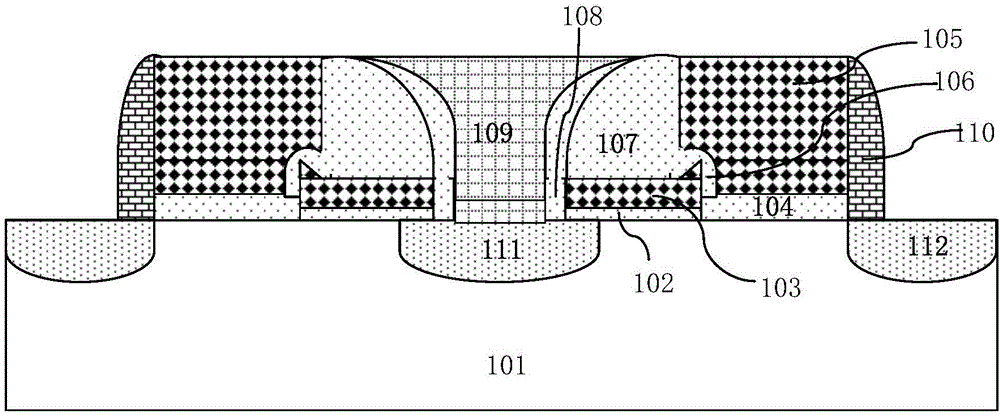
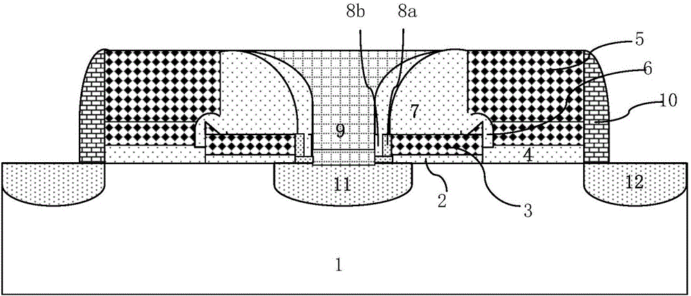
[0064] Such as figure 2 Shown is a schematic cross-sectional view of a cell structure of a self-aligned split-gate flash memory device according to an embodiment of the present invention. The cell structure of a self-aligned split-gate flash memory device according to an embodiment of the present invention includes: formed on a P-type doped semiconductor substrate such as silicon Polysilicon word line 5 , polysilicon floating gate 3 and source polysilicon 9 on substrate 1 .

[0065] The second side of the polysilicon floating gate 3 has an inclined structure with gradually increasing thickness, the thickness of the polysilicon word line 5 is greater than the thickness of the polysilicon floating gate 3, and the first side of the polysilicon word line 5 is tunneled. The oxide layer 6 covers the second side of the polysilicon floating gate 3 from the side and extends to the top of the second side of the polysilicon floating gate 3 .

[0066] The first floating gate spacer 7 co...


PUM


Abstract

The invention discloses a self-aligned split gate flash memory device. One unit structure comprises a polysilicon word line, a polysilicon floating gate and source polysilicon, wherein a first floating gate sidewall covers a top surface of the polysilicon floating gate and a first side surface of the polysilicon word line; a second floating gate sidewall is formed on the first side surface of the polysilicon floating gate; the first floating gate sidewalls and the second floating gate sidewalls of two adjacent unit structures define a forming region of the source polysilicon in a self-aligned manner and the width of the bottom of the source polysilicon is defined by each second floating gate sidewall in a self-aligned manner; a second floating gate sidewall material comprises a first oxide layer and a second oxide layer formed by CVD HTO; and the first oxide layer is formed by carrying out thermal oxidation on silicon on the first side surface of the polysilicon floating gate. The invention further discloses a manufacturing method of the self-aligned split gate flash memory device. According to the self-aligned split gate flash memory device and the manufacturing method thereof, the data retention capacity of the device can be improved and good control on the width of the bottom of the source polysilicon and the length of the polysilicon floating gate can be ensured.

Description

technical field [0001] The invention relates to a semiconductor integrated circuit manufacturing method, in particular to a self-aligned split-gate flash memory device; the invention also relates to a self-aligned split-gate flash memory device manufacturing method. Background technique [0002] Such as figure 1 Shown is a schematic cross-sectional view of a cell structure of an existing self-aligned split-gate flash memory device. Taking an N-type device as an example, the cell structure of an existing self-aligned split-gate flash memory device is formed on a P-type doped semiconductor substrate such as On the silicon substrate 101, a coupling oxide layer 102, a polysilicon floating gate (FG) 103, a gate oxide layer 104 and a polysilicon word line 105 are formed on the surface of the semiconductor substrate 101; [0003] A tunnel oxide layer 106 is isolated between the second side of the polysilicon floating gate 103 and the bottom of the first side of the polysilicon wor...

Claims


Application Information

Patent Timeline
Patent Type & Authority Applications(China)
IPC IPC(8): H01L27/115H01L21/8247H01L29/788
CPCH01L29/788H10B41/00H10B41/30
Inventor 林益梅
Owner SHANGHAI HUAHONG GRACE SEMICON MFG CORP
Why Eureka
Try Eureka