High electron mobility transistor device and manufacturing method thereof

A high electron mobility, manufacturing method technology, applied in semiconductor/solid state device manufacturing, semiconductor devices, electrical components, etc., can solve the problem of reducing the reliability of high electron mobility transistor 002, T-type gate 232 and source field plate 020 Short circuit, dielectric layer 010 is prone to failure, etc., to reduce the probability of failure, weaken the strong electric field, and improve reliability.

Active Publication Date: 2017-01-04
昆山工研院第三代半导体研究院有限公司
View PDF4 Cites 16 Cited by
  • Summary
  • Abstract
  • Description
  • Claims
  • Application Information

AI Technical Summary

Problems solved by technology

When the high electron mobility transistor 002 works under long-term stress and high-voltage stress, there is a long-term high electric field between the T-shaped gate 232 and the source field plate 020, which makes the dielectric layer 010 on the side wall of the step 030 very prone to Failure, resulting in a short circuit between the T-shaped gate 232 and the source field plate 020, thereby reducing the reliability of the high electron mobility transistor 002
[0006] In view of the above-mentioned HEMT using the conventional source field plate technology, there is a problem that the reliability of the device is reduced due to the failure of the dielectric layer between the gate and the source field plate, and it is necessary to provide a highly reliable HEMT and its manufacturing method

Method used


Image

  • High electron mobility transistor device and manufacturing method thereof
  • High electron mobility transistor device and manufacturing method thereof
  • High electron mobility transistor device and manufacturing method thereof

Examples


no. 1 example

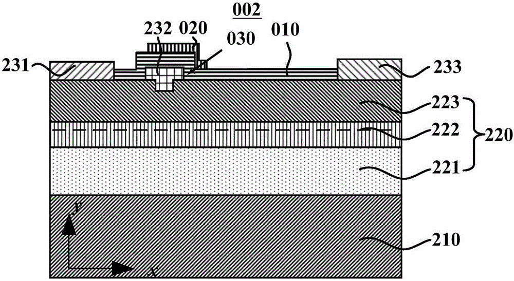
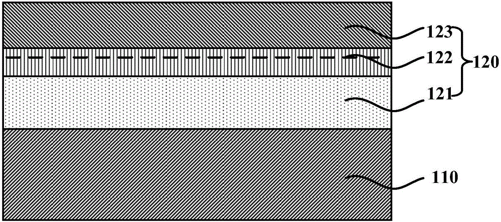
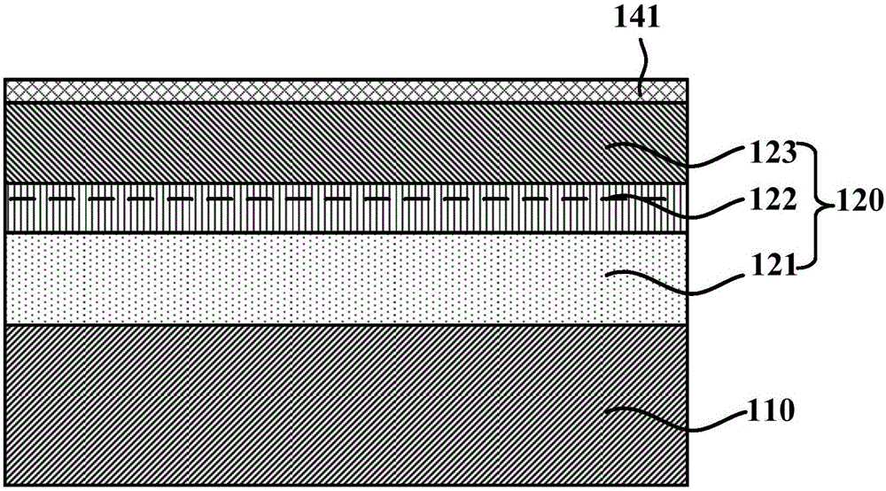
[0049] 2, the present embodiment provides a high electron mobility transistor device 100, which includes: a substrate 110, a semiconductor layer 120, a gate 132, a source 131, a drain 133, a first dielectric layer 141, a second A source field plate 151 , a second dielectric layer 142 , and a second source field plate 152 , wherein the source electrode 131 , the first source field plate 151 and the second source field plate 152 are at the same potential. The semiconductor layer 120 is located on the substrate 110 , specifically on the upper surface of the substrate 110 ; the gate 132 , the source 131 and the drain 133 are located on the semiconductor layer 120 , and the gate 132 is located between the source 131 and the drain 133 . In this embodiment, both the source 131 and the drain 133 are located on the upper surface of the semiconductor layer 120 and are in contact with the semiconductor layer 120 , and the bottom end of the gate 132 is embedded in the semiconductor layer 1...

no. 2 example

[0075] Please refer to image 3 , the present embodiment provides a high electron mobility transistor device 200, which has approximately the same structure as the high electron mobility transistor device 100 provided in the first embodiment, and the second source field plate 152 is in contact with the source electrode 131 (electrically connected) , the difference between the two is that in this embodiment, the second dielectric layer 142 on the first source field plate 151 is provided with a through hole 170, and the part of the second source field plate 252 on the first source field plate 151 passes through the through hole 170. The hole 170 is in contact with the first source field plate 151 , that is, the second source field plate 252 is electrically connected to the first source field plate 151 , so as to realize the equipotential of the source 131 , the first source field plate 151 and the second source field plate 152 .

[0076] The first source field plate 151 and the ...

no. 3 example

[0079] Please refer to Figure 4 , this embodiment provides a high electron mobility transistor device 300, which has substantially the same structure as the high electron mobility transistor device 100 provided in the first embodiment, and the first source field plate 151 and the source electrode 131 are electrically connected outside the active region. The difference between the two is that in this embodiment, the second source field plate 352 is only located on the gate 132 and the second dielectric layer 142 on the first source field plate 151, and the second source field plate 352 and the active The outer region is electrically connected to realize the equipotential of the source 131 , the first source field plate 151 and the second source field plate 352 .

[0080] The first source field plate 151 and the second source field plate 352 in this embodiment weaken the strong electric field between the gate 132 and the drain 133 close to the gate 132 and at the same time the ...


PUM


Abstract

The invention provides a high electron mobility transistor device, relating to the technical field of semiconductors. The first dielectric layer of the device is on a semiconductor layer between a gate and source and drain electrodes. A first source field plate is on the first dielectric layer between the gate and the drain electrode. A second dielectric layer is on the gate, the first source field plate and the first dielectric layer. A second source field plate is on the gate and the first source field plate. The first source field plate and the second source field plate weaken the strong electric field close to a gate area between the gate and the drain electrode. The probability of the failure of the first dielectric layer and the second dielectric layer under long-time stress and high voltage stress is little. According to the device, the strong electric field close to the gate area between the gate and the drain electrode can be weakened, and the probability of the failure of the dielectric layers between the gate and the source field plates can be reduced. The invention also provides a manufacturing method of the high electron mobility transistor device, the process is simple, and the reliability of the manufactured device is high.

Description

technical field [0001] The invention relates to the technical field of semiconductors, in particular to a high electron mobility transistor device and a manufacturing method thereof. Background technique [0002] The dielectric breakdown electric field of the third-generation semiconductor gallium nitride (GaN) is much higher than that of the first-generation semiconductor silicon (Si) or the second-generation semiconductor gallium arsenide (GaAs), and its value is as high as 3MV / cm , so that the electronic device can withstand very high voltage. At the same time, gallium nitride can form a heterojunction structure with other gallium-based compound semiconductors (eg, Group III nitride semiconductors). Since group III nitride semiconductors have strong spontaneous polarization and piezoelectric polarization effects, they can form a two-dimensional electron gas (2DEG) channel with a high electron concentration near the interface of the heterojunction, and this heterostructur...

Claims


Application Information

Patent Timeline
Patent Type & Authority Applications(China)
IPC IPC(8): H01L29/40H01L29/778H01L21/335
Inventor 尹成功裴轶
Owner 昆山工研院第三代半导体研究院有限公司
Why Eureka
Try Eureka