Method for metalizing aluminide substrate through laser light and aluminide substrate

An aluminide and metallization technology, applied in the field of microelectronics, can solve problems such as high cost and complex process, and achieve the effects of low cost, uniform laser energy distribution, and uniform metal thickness

Inactive Publication Date: 2017-01-11
INST OF SEMICONDUCTORS - CHINESE ACAD OF SCI
View PDF6 Cites 7 Cited by
  • Summary
  • Abstract
  • Description
  • Claims
  • Application Information

AI Technical Summary

Problems solved by technology

[0006] In order to solve the above-mentioned problem of complex process and high cost in metallization of aluminum nitride ceramics, the present invention provides a technical solution for metallization of aluminide substrates by laser

Method used


Image

  • Method for metalizing aluminide substrate through laser light and aluminide substrate
  • Method for metalizing aluminide substrate through laser light and aluminide substrate

Examples


Embodiment Construction

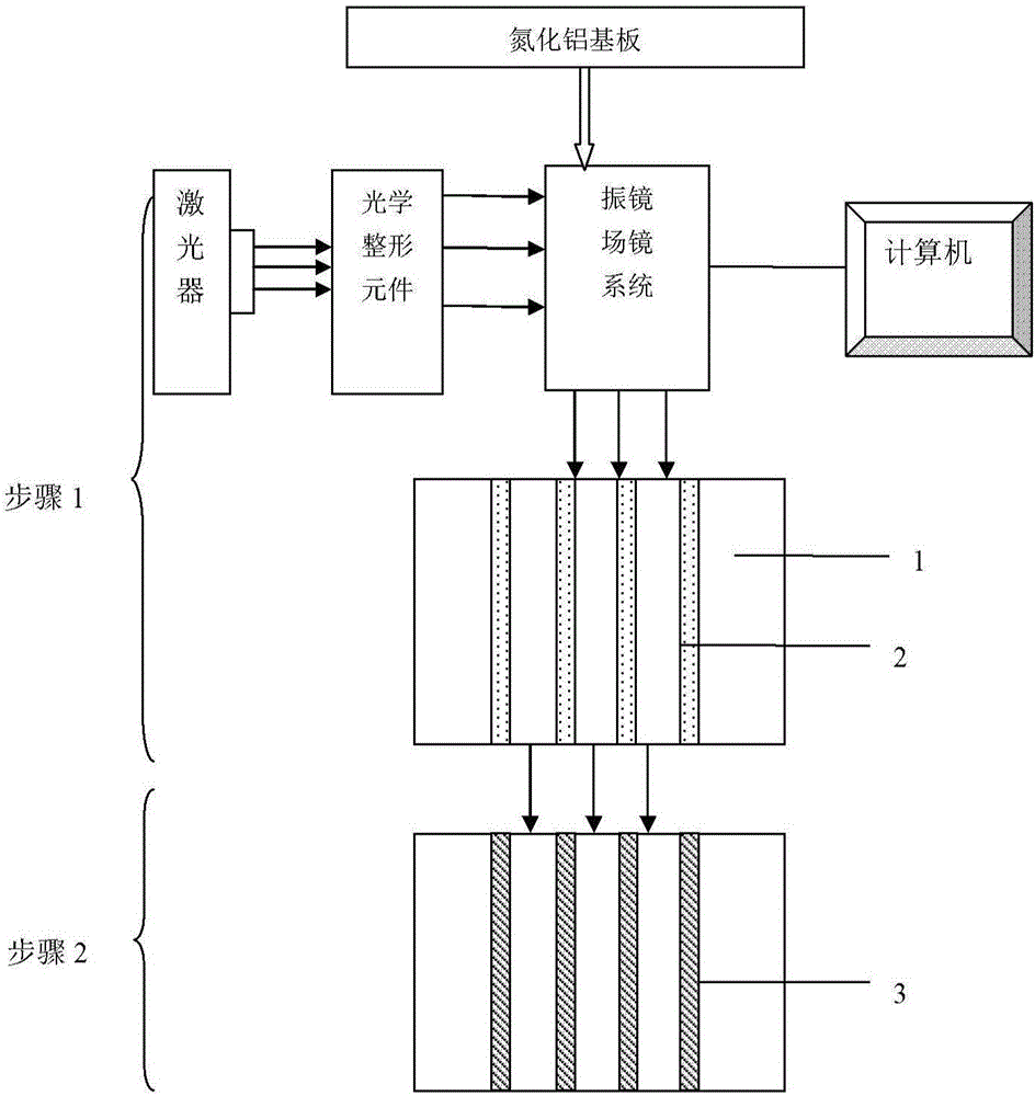
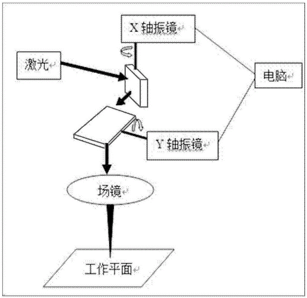
[0022] The invention modulates the phase of laser light through an optical shaping element based on binary optics to obtain flat-top light, and then the flat-top light is focused and irradiated onto the aluminide substrate through a galvanometer field mirror system. The ultra-high temperature generated by the laser decomposes the aluminide into metallic aluminum, so that aluminum wires with specific shape, size and distribution on the surface of the aluminide can be obtained. Then electroplating or electroless plating is used to metallize the conductive aluminum surface, and the area that has not been treated by laser is not metallized, and the aluminum wire is directly realized on the aluminide substrate by using a computer-controlled galvanometer scanning method to realize the patterning of the metal electrode. .

[0023] Specifically, the present invention provides a method for laser metallizing an aluminide substrate. The specific steps include: step 1, laser treatment of ...


PUM

PropertyMeasurementUnit
wavelengthaaaaaaaaaa

Abstract

The invention discloses a method for metalizing an aluminide substrate through laser light and the corresponding aluminide substrate. Phase modulation is conducted on the laser light through an optical shaping element based on binary optics, so that flat-topped light is obtained, and the flat-topped light is irradiated onto the aluminide substrate in a focused mode through a galvanometer field lens system. Metallic aluminum is separated from aluminide through ultrahigh temperature generated by the laser light, so that an aluminum wire in a specific shape and of a specific size and distribution form on the aluminide surface is obtained; and then the conductive aluminum surface is metalized through an electroplating method or a chemical plating method. The area which is not subjected to laser light treatment is not metalized, the aluminum wire is directly formed on the aluminide substrate in the way that a computer is used for controlling galvanometer scanning, and accordingly patterning of a metal electrode is achieved. Compared with a traditional aluminide substrate metalizing method, the method for metalizing the aluminide substrate through laser light and the corresponding aluminide substrate have the advantages that the technique is simpler, the cost is lower, and patterning of the metal electrode can be achieved directly; and in addition, by using the optic shaping element, distribution of laser energy is made uniform, and the obtained metal thickness is also uniform.

Description

technical field [0001] The invention relates to the technical field of microelectronics, in particular to a metallization method for an aluminide substrate of a high-power device and an aluminide substrate produced by the method. Background technique [0002] With the rapid development of power devices, the heat generated by the devices also increases rapidly. Aluminum nitride ceramics have excellent thermal conductivity and insulation properties, and also have the characteristics of low dielectric constant and thermal expansion coefficient close to chip materials, and are ideal heat dissipation substrates and packaging materials for large-scale integrated circuits. [0003] When packaging electronic devices, it is necessary to prepare a layer of metal on aluminum nitride ceramics first, and then contact the chip with aluminum nitride ceramics. Therefore, the metallization process of aluminum nitride ceramics is a crucial link in the entire packaging process. one. Traditio...

Claims


Application Information

Patent Timeline
Patent Type & Authority Applications(China)
IPC IPC(8): B23K26/00
CPCB23K26/00B23K2103/10
Inventor 王晓峰王帅刘敏杨富华
Owner INST OF SEMICONDUCTORS - CHINESE ACAD OF SCI
Why Eureka
Try Eureka