OLED display device and fabrication method thereof

A technology for a display device and a manufacturing method, which is applied in the manufacture of semiconductor/solid-state devices, electrical components, and electrical solid-state devices, etc., can solve problems such as device failure, and achieve the effects of improving adhesion, increasing contact area, and reducing the probability of falling off.

Active Publication Date: 2017-01-11
WUHAN CHINA STAR OPTOELECTRONICS TECH CO LTD
View PDF4 Cites 40 Cited by
  • Summary
  • Abstract
  • Description
  • Claims
  • Application Information

AI Technical Summary

Problems solved by technology

[0004] Studies have shown that water vapor and oxygen will have a great impact on the performance of OLED devices. One is that water vapor and oxygen may react with the cathode material of silver (Ag) and magnesium (Mg); the other is that water vapor and oxygen may react with air. A chemical reaction occurs between the hole transport layer and the electron transport layer, causing device failure

Method used


Image

  • OLED display device and fabrication method thereof
  • OLED display device and fabrication method thereof
  • OLED display device and fabrication method thereof

Examples


Embodiment Construction

[0031] In order to further illustrate the technical means adopted by the present invention and its effects, the following describes in detail in conjunction with preferred embodiments of the present invention and accompanying drawings.

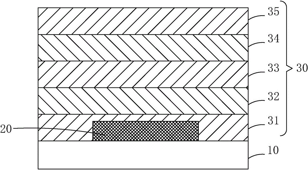
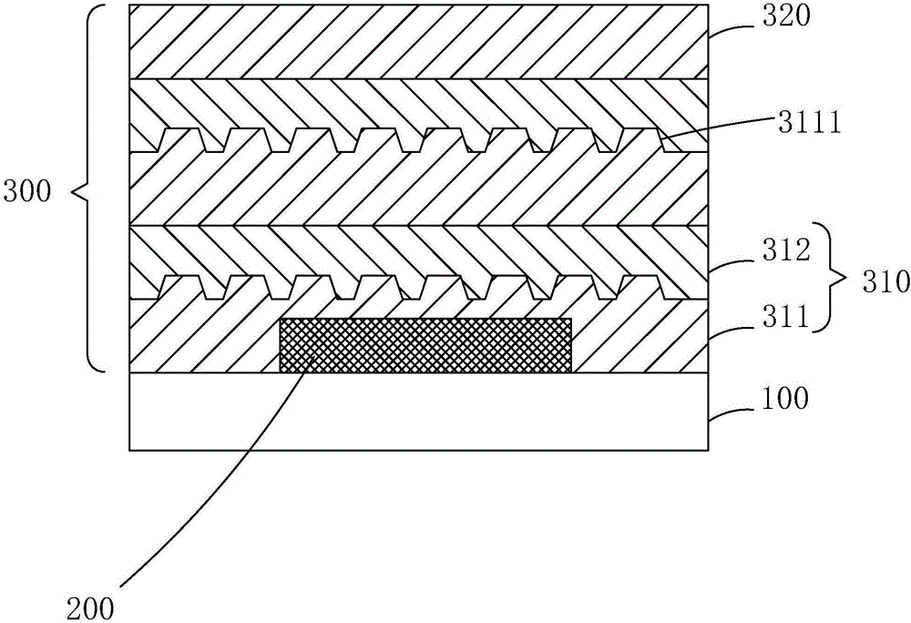
[0032] see figure 2 , the present invention provides an OLED display device, comprising a substrate 100, an OLED device 200 disposed on the substrate 100, and a thin film encapsulation layer 300 disposed on the OLED device 200 and the substrate 100 and covering the OLED device 200 ;

[0033] The thin-film encapsulation layer 300 includes a plurality of intermediate encapsulation units 310 stacked, and a top inorganic barrier layer 320 disposed on the uppermost intermediate encapsulation unit 310, each intermediate encapsulation unit 310 includes an intermediate inorganic barrier layer 311, and an organic buffer layer 312 disposed on the intermediate inorganic barrier layer 311;

[0034] In the thin film encapsulation layer 300, the upper su...


PUM


Abstract

The invention provides an OLED display device and the fabrication method thereof. The invention uses a mask with multiple openings as the cover to form the middle inorganic blocking layer in the film encapsulation layer, making the upper surface of the middle inorganic blocking layer has many evenly distributed bulges, greatly increasing the contact area between the organic buffer layer covered on the middle inorganic blocking layer and the middle inorganic blocking layer, thus increasing the adhesive force between the middle inorganic blocking layer and the organic buffer layer at the interface and greatly reducing the probability the partition between the inorganic blocking layer and the organic buffer layer. The bulges can prevent water and oxygen molecules from moving on the interface between the middle inorganic blocking layer and the organic buffer layer and prevent water and oxygen molecules from continuing to intrude into the internal part of the OLED display device, which will influence efficiency of the components of OLED.

Description

technical field [0001] The invention relates to the field of display technology, in particular to an OLED display device and a manufacturing method thereof. Background technique [0002] In recent years, flat panel display devices such as Liquid Crystal Display (LCD) devices and Organic Light Emitting Diode (OLED) display devices have gradually replaced CRT displays and become mainstream products in the display device market. Among them, OLED display devices have many advantages such as self-illumination, low driving voltage, high luminous efficiency, short response time, high definition and contrast, near 180° viewing angle, wide operating temperature range, flexible display and large-area full-color display, etc. , is recognized by the industry as the most promising display device. [0003] An OLED display device generally includes: a substrate, an encapsulation cover plate disposed opposite to the substrate, an anode disposed on the substrate, a hole injection layer disp...

Claims


Application Information

Patent Timeline
Patent Type & Authority Applications(China)
IPC IPC(8): H01L51/52H01L51/56
CPCH10K50/8445H10K50/844H10K71/00
Inventor 王杲祯余威
Owner WUHAN CHINA STAR OPTOELECTRONICS TECH CO LTD
Why Eureka
Try Eureka