
Flexible circuit board and manufacturing method thereof
A technology of flexible circuit boards and manufacturing methods, which is applied in the manufacture of printed circuits, removal of conductive materials by chemical/electrolytic methods, printed circuits, etc., can solve problems such as monopoly and high material costs, and achieve ultra-low loss signal transmission, reduce Manufacturing cost, effect of improving transmission quality
Patent Information
- Authority / Receiving Office
- CN · China
- Patent Type
- Applications(China)
- Current Assignee / Owner
- Publication Date
- 2017-01-11
Smart Images
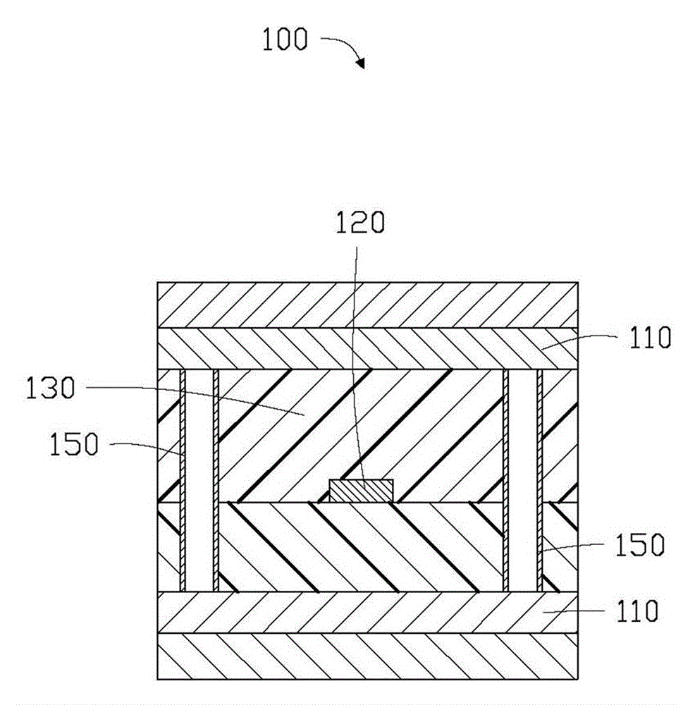
Figure 1 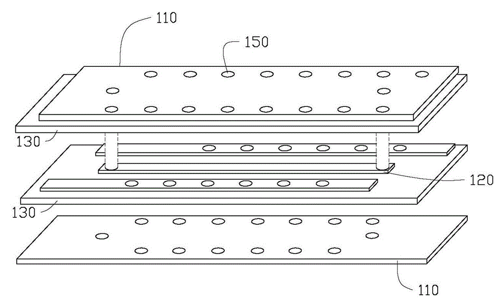
Figure 2 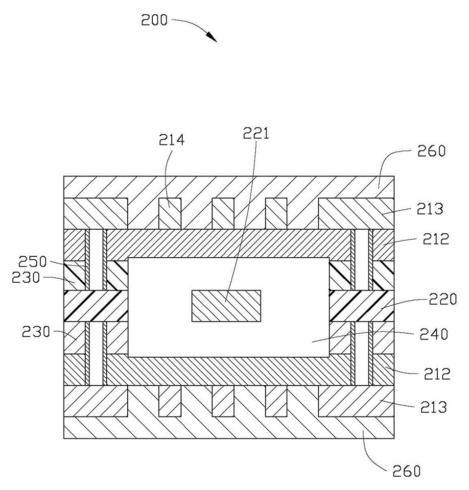
Figure 3
Abstract
Description
Technical field
[0001] The invention relates to a printed circuit board technology, in particular to a flexible circuit board and a manufacturing method of the flexible circuit board. Background technique
[0002] figure 1 It is a schematic cross-sectional view of a conventional high-frequency signal line structure 100. The high-frequency signal line structure 100 includes two ground pattern layers 110, one signal line 120, two dielectric layers 130 and a plurality of conductive holes 150. Wherein, the dielectric layer 130 completely covers the signal line 120 so that the signal line 120 is disposed between the two ground pattern layers 110.
[0003] figure 2 for figure 1 A layered three-dimensional schematic diagram of the mid- and high-frequency signal line structure 100. The conductive holes 150 are equidistantly distributed on both sides of the signal line 120 and conduct the ground pattern layers 110. In other words, through the plurality of ground pattern layers 110, the p...
Examples
Embodiment Construction
[0027] In order to further explain the technical means and effects adopted by the present invention to achieve the intended purpose of the invention, the specific implementation, structure, features and effects of the flexible circuit board and its manufacturing method of the present invention will be detailed below with reference to the drawings and preferred embodiments. described as follows.
[0028] The first embodiment of the present invention discloses a flexible circuit board 200 that uses air as a dielectric layer to cover the linear signal line 221 so that the linear signal line 221 is in a suspended state. See image 3 As shown, it is a schematic cross-sectional view of the flexible circuit board 200. Figure 4 Is a schematic diagram of the flexible circuit board 200 from the inside to the outside of the circuit pattern, adhesive glue and copper-clad substrate, Figure 5 Middle (A)-(F) are schematic cross-sectional views of each step of the manufacturing method of the fl...