Formation method of semiconductor device

A semiconductor and device technology, applied in the field of semiconductor device formation, can solve problems such as electrical performance needs to be improved, and achieve the effect of improving electrical performance

Active Publication Date: 2017-01-18
SHANGHAI HUAHONG GRACE SEMICON MFG CORP
View PDF2 Cites 7 Cited by
  • Summary
  • Abstract
  • Description
  • Claims
  • Application Information

AI Technical Summary

Problems solved by technology

[0005] However, the electrical performance of semiconductor devices including reference cell devices and split-gate devices formed in the prior art needs to be improved

Method used


Image

  • Formation method of semiconductor device
  • Formation method of semiconductor device
  • Formation method of semiconductor device

Examples


Embodiment Construction

[0022] It can be seen from the background art that the electrical performance of semiconductor devices including reference cell devices and split-gate devices in the prior art needs to be improved.

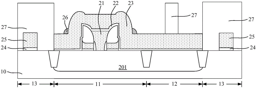
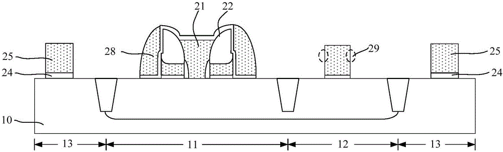
[0023] Now combine the formation process of a semiconductor device for research, figure 1 and figure 2 It is a schematic cross-sectional structure diagram of the formation process of a semiconductor device. During the formation process of the semiconductor device, the reference unit gate of the reference unit device and the word line of the split-gate device are formed by the same photolithography process.

[0024] refer to figure 1 , providing a substrate 10, the substrate 10 includes a flash memory area 11, a reference cell area 12 and a logic area 13; a separate flash gate (not marked) is formed on the substrate 10 of the flash memory area 11, and is located in an adjacent flash memory The source gate 21 between the gates; the tunnel dielectric layer 22 is formed on the subs...


PUM


Abstract

The invention discloses a formation method of a semiconductor device. The method comprises the following steps: forming a tunneling dielectric layer on a substrate of a flash memory area, a reference unit zone and a logic zone, wherein the tunneling dielectric layer is also disposed on a flash memory grid and a source grid; forming a word line layer on the tunneling dielectric layer; forming a first photoresist layer on the word line layer of the flash memory zone and a part of the word line layer of the reference unit zone; by taking the first photoresist layer as a mask layer, removing the word line layer disposed on the logic zone through etching, and also removing the word line layer exposed on the reference unit zone through etching, wherein the residual word line layer on the reference unit zone is used for forming a reference unit grid; after the reference unit grid is formed, forming a logic grid on the substrate of the logic zone; forming a second photoresist layer on the logic grid and the reference unit grid; and after the second photoresist layer is formed, etching the word line layer of the flash memory zone, and forming a word line on the substrate of the flash memory zone. According to the invention, the morphology of the reference unit grid of a reference unit device is improved, and electrical performance of the formed semiconductor device is improved.

Description

technical field [0001] The invention relates to the technical field of semiconductor manufacturing, in particular to a method for forming a semiconductor device. Background technique [0002] In the current semiconductor industry, storage devices account for a considerable proportion of integrated circuit products, and the development of flash memory in memory is particularly rapid. Its main feature is that it can keep the stored information for a long time without power on. It has many advantages such as high integration, fast access speed and easy erasure, so it has been widely used in many fields such as microcomputer and automatic control. widely used. [0003] Flash memories are classified into two types: stack gate devices and split gate devices. The stacked gate device has a floating gate and a control gate, wherein the control gate is located above the floating gate. The method for manufacturing the stacked gate device is simpler than the method for manufacturing t...

Claims


Application Information

Patent Timeline
Patent Type & Authority Applications(China)
IPC IPC(8): H01L27/11517
CPCH10B41/00
Inventor 王卉曹子贵陈宏徐涛
Owner SHANGHAI HUAHONG GRACE SEMICON MFG CORP
Why Eureka
Try Eureka