Novel uncooled infrared focal plane detector pixel and fabrication method thereof

A focal plane detector and uncooled infrared technology, which is applied in the manufacture of electrical components, semiconductor devices, final products, etc., can solve the problem of limited resonant cavity height, limited infrared wavelength range, and inability to meet the pixel requirements of high absorption rate detectors, etc. problem, achieve the effect of preventing breakage or warping

Inactive Publication Date: 2017-01-18
YANTAI RAYTRON TECH
View PDF6 Cites 11 Cited by
  • Summary
  • Abstract
  • Description
  • Claims
  • Application Information

AI Technical Summary

Problems solved by technology

However, as the pixel size shrinks, this structure will not be able to meet the needs of high-absorption detector pixels
In addition, due to the limited hei

Method used


Image

  • Novel uncooled infrared focal plane detector pixel and fabrication method thereof
  • Novel uncooled infrared focal plane detector pixel and fabrication method thereof
  • Novel uncooled infrared focal plane detector pixel and fabrication method thereof

Examples


Embodiment Construction

[0074] The principles and features of the present invention are described below in conjunction with the accompanying drawings, and the examples given are only used to explain the present invention, and are not intended to limit the scope of the present invention.

[0075] A method for manufacturing a novel uncooled infrared focal plane detector pixel, comprising the following steps:

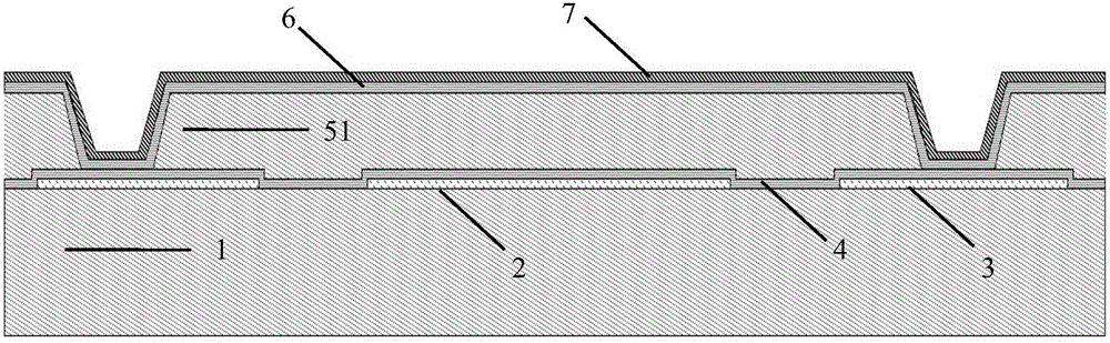
[0076] Step 1: If figure 1 As shown, a semiconductor substrate 1 comprising a readout circuit (not shown) is provided, a metal layer is deposited on the semiconductor substrate 1; and the metal layer is patterned to form a metal reflective layer 2 pattern and a metal electrode Block 3, the thickness of the metal reflective layer 2 is 0.05-0.40 μm; the metal electrode block 3 is electrically connected to the readout circuit on the semiconductor substrate 1; an insulating dielectric layer 4 is deposited on the patterned metal layer, and the insulating dielectric layer 4 is Silicon nitride film or ...


PUM

PropertyMeasurementUnit
Thicknessaaaaaaaaaa
Thicknessaaaaaaaaaa
Thicknessaaaaaaaaaa

Abstract

The invention discloses a novel uncooled infrared focal plane detector pixel and a fabrication method thereof and belongs to the uncooled infrared focal plane detector technical field. The novel uncooled infrared focal plane detector pixel comprises three layers of structures which are located on a semiconductor substrate sequentially from bottom to top, wherein the first layer of bridge structure includes a metal reflection layer, an insulating dielectric layer, a first supporting layer, a first supporting layer protection layer, a first metal electrode layer and a first silicon nitride dielectric layer, the second layer of thermal conversion structure includes a second supporting layer, a second supporting layer protection layer, a second metal electrode layer, a second silicon nitride dielectric layer, a thermal sensitive layer and a heat sensitive layer protection layer, and the third layer of absorption structure includes a third supporting layer, an absorption layer and an absorption protection layer. The invention also discloses a fabrication method of the novel uncooled infrared focal plane detector pixel. With the novel uncooled infrared focal plane detector pixel provided by the invention adopted, the absorption rate of infrared radiation can be obviously improved, the response rate of a detector can be improved, and a foundation can be laid for the manufacture of larger-array and smaller-pixel detectors.

Description

technical field [0001] The invention relates to a novel uncooled infrared focal plane detector pixel and a manufacturing method thereof, belonging to the technical field of the uncooled infrared focal plane detector. Background technique [0002] With the gradual reduction of pixel size, the target radiation energy absorbed by a single sensor is significantly reduced. In order to maintain a relatively consistent sensor sensitivity, the sensor's responsivity must be increased. The responsivity of the sensor depends on the pixel size, the thermal conductance between the sensor and the substrate, the optical absorption efficiency of the sensor and the performance of the heat-sensitive material. In the traditional double-layer microbridge structure, the first layer is a bridge leg support structure composed of slender bridge legs, which is used to improve the thermal conduction between the sensor and the substrate. The second layer consists of a vanadium oxide layer that absor...

Claims


Application Information

Patent Timeline
IPC IPC(8): H01L31/09H01L31/18
CPCH01L31/09H01L31/18Y02P70/50
Inventor 王宏臣邱栋王鹏陈文礼
Owner YANTAI RAYTRON TECH
Why Eureka
Try Eureka