Film plating device for preparing TCO (Transparent Conductive Oxide) film and film plating method

An oxide thin film, transparent oxide technology, applied in circuits, photovoltaic power generation, electrical components, etc., can solve the problems of low coating quality and high coating cost, achieve high-speed deposition rate and reduce damage.

Active Publication Date: 2017-01-18
ZHONGWEI NEW ENERGY CHENGDU CO LTD
View PDF3 Cites 9 Cited by
  • Summary
  • Abstract
  • Description
  • Claims
  • Application Information

AI Technical Summary

Problems solved by technology

[0009] In view of the shortcomings of the prior art described above, the purpose of the present invention is to provide a coating device and a coating method for making a transparent conductive oxide film, which is used to solve the problems of low coating quality and high coating cost in the prior art

Method used


Image

  • Film plating device for preparing TCO (Transparent Conductive Oxide) film and film plating method
  • Film plating device for preparing TCO (Transparent Conductive Oxide) film and film plating method
  • Film plating device for preparing TCO (Transparent Conductive Oxide) film and film plating method

Examples


Embodiment 1

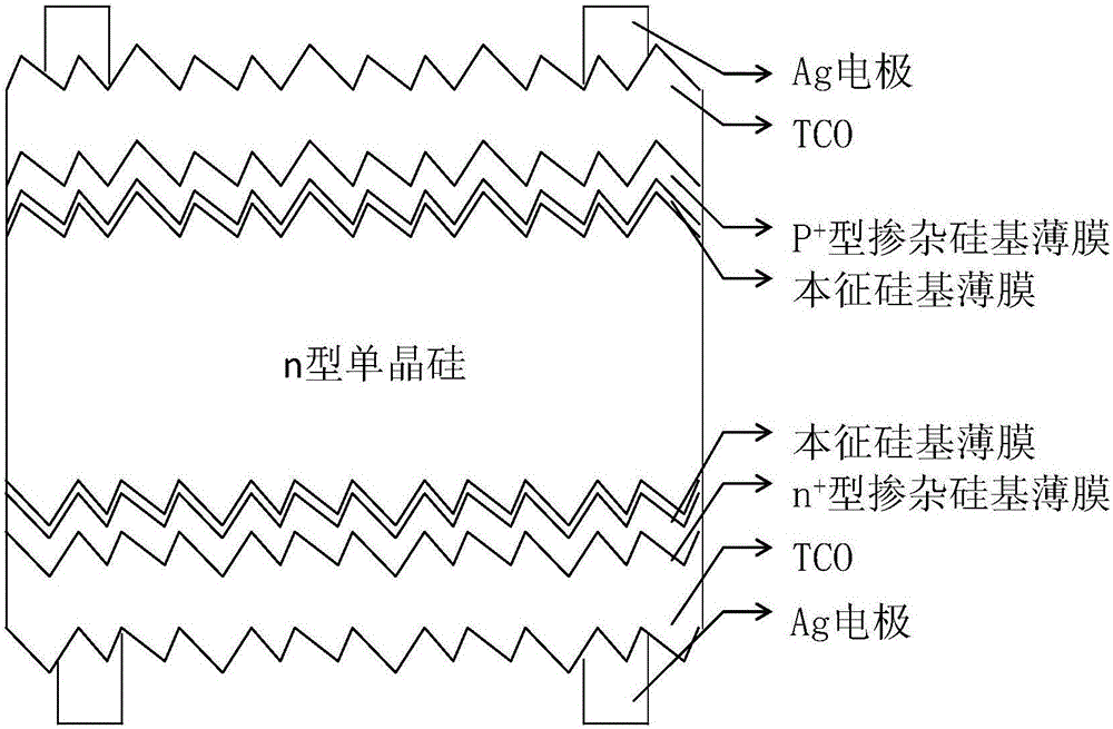
[0044] This embodiment describes the equipment and method for continuously fabricating low-damage, high-quality TCO thin film stacks on the light-receiving front surface of a photoelectric conversion device or solar cell.

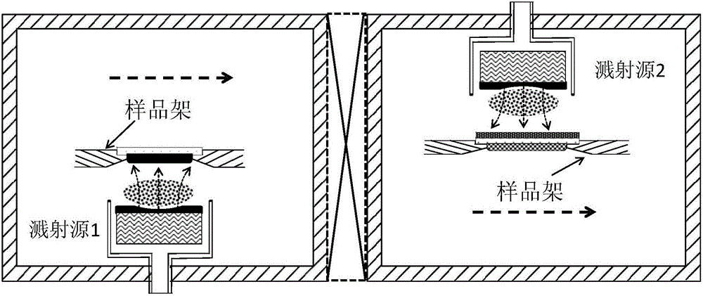
[0045] see Figure 6 , which is a schematic structural view of the coating equipment used in this embodiment for producing a transparent conductive oxide thin film. The equipment consists of two parts, the ion coating source and the sputtering coating source, which are respectively installed in two independent vacuum chambers, and the two chambers are separated by a diaphragm valve. The coating direction of the ion coating source and the sputtering coating source are the same, and TCO thin film stacks of different materials or TCO thin film stacks of the same material with different structures can be continuously produced under different vacuum and gas atmosphere conditions by moving the sample holder.

[0046] In one case, the ion-plating source can be us...

Embodiment 2

[0056] This embodiment describes the equipment and method for continuously fabricating TCO thin films or thin film stacks on both sides of photoelectric conversion devices or solar cells.

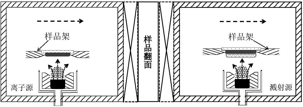
[0057] see Figure 7 , which is a schematic structural view of the coating equipment used in this embodiment for producing a transparent conductive oxide thin film. The equipment consists of two parts, an ion coating source and a sputtering coating source. The coating directions of the ion coating source and the sputtering coating source are opposite, and they are respectively installed in two independent vacuum chambers. The two chambers are separated by a partition The plate valve is separated, and the TCO film can be prepared on the front surface and the back surface of the photoelectric conversion device or solar cell in sequence without exposing the atmosphere, so as to avoid the increase of the device structure caused by the flipping of the device and the impact on the photoelectric c...

Embodiment 3

[0065] The difference between this embodiment and the second embodiment is that the sputtering coating source is combined with a radio frequency sputtering coating source and a direct current sputtering coating source.

[0066] see Figure 8 , which is a schematic structural view of the coating equipment used in this embodiment for producing a transparent conductive oxide thin film. The equipment consists of two parts, the ion coating source and the sputtering coating source, which are respectively installed in two independent vacuum chambers, and the two chambers are separated by a diaphragm valve.

[0067] As an example, the ion coating source is an RPD coating source, the coating direction is from bottom to top, the target material is tungsten-doped indium oxide (IWO), and the doping concentration of tungsten oxide is 3%.

[0068] As an example, the sputtering coating source is combined with a radio frequency sputtering coating source and a DC sputtering coating source, th...


PUM

PropertyMeasurementUnit
thicknessaaaaaaaaaa
thicknessaaaaaaaaaa
thicknessaaaaaaaaaa

Abstract

The invention provides a film plating device for preparing a TCO film and a film plating method. The film plating device integrates an ion film plating source with a sputtering film plating source in the same vacuum equipment. Characteristics of ion film plating and sputtering film plating are combined effectively, TCO films of different optical and electrical properties are prepared continuously under the condition that the films are not exposed in the atmosphere according to different requirements for the TCO films of devices, a high deposition speed is obtained, and damage on a substrate and the device surface caused in the film deposition process is reduced. The device and method are especially suitable for preparing the TCO films continuously in the front and back sides of high-efficiency film silicon/crystalline silica heterojunction solar cells with low loss as well as preparing different TCO films continuously in different film solar cells; and the device and method are suitable for different TCO materials with different performances.

Description

technical field [0001] The invention belongs to the field of film preparation, and relates to a film coating device and a film coating method for making a transparent conductive oxide film. Background technique [0002] A photoelectric converter is a semiconductor device that receives light and generates an electrical signal. In order to improve the absorption efficiency of photoelectric conversion devices for incident light, an optical film that reduces light reflection, that is, an anti-reflection film, is usually fabricated on the surface of the device receiving light irradiation, which corresponds to Anti Reflection Coating in English, or ARC film for short. In order to improve the device’s collection efficiency of photogenerated carriers, a transparent conductive oxide film (TCO film) with high light transmittance and good conductivity is usually used as a surface anti-reflection film, that is, a transparent conductive anti-reflection film. The solar cell is also a pho...

Claims


Application Information

Patent Timeline
Patent Type & Authority Applications(China)
IPC IPC(8): H01L31/18H01L31/0216H01L21/67H01L21/3205
CPCH01L21/3205H01L21/67011H01L31/02168H01L31/1804Y02E10/547Y02P70/50
Inventor 刘正新孟凡英石建华
Owner ZHONGWEI NEW ENERGY CHENGDU CO LTD
Why Eureka
Try Eureka