Gas sensor, array and a method for manufacturing thereof

A gas sensor and sensor technology, which can be used in the structural details of gas analyzers, semiconductor/solid-state device manufacturing, and electrical solid-state devices, etc., and can solve problems such as inapplicable and unsuitable gas sensors.

Pending Publication Date: 2017-02-15
SENSIRION AG
View PDF7 Cites 1 Cited by
  • Summary
  • Abstract
  • Description
  • Claims
  • Application Information

AI Technical Summary

Problems solved by technology

Conventional annealing steps, such as exposing the semiconductor chip to the heat generated in a furnace, may not be suitable for

Method used


Image

  • Gas sensor, array and a method for manufacturing thereof
  • Gas sensor, array and a method for manufacturing thereof
  • Gas sensor, array and a method for manufacturing thereof

Examples


Embodiment Construction

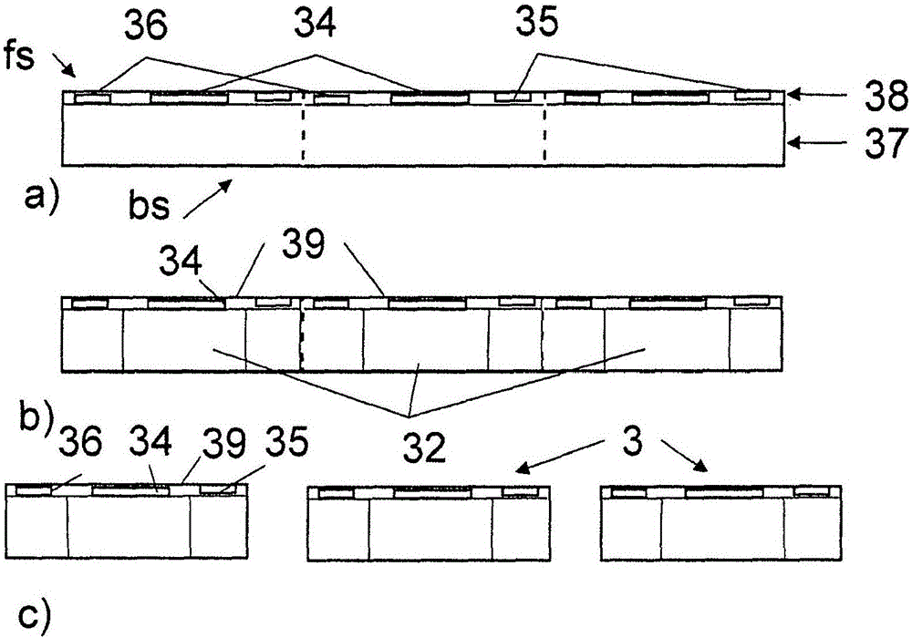
[0038] figure 1 Manufacturing steps applied in a method of manufacturing a gas sensor according to an embodiment of the present invention are shown in schematic diagrams a) to c). These steps refer to the fabrication of a suitable gas sensor chip that will later be packaged into the gas sensor. in gesture figure 1 In a), a wafer is provided which contains a semiconductor substrate 37 and a layer stack 38 arranged on the semiconductor substrate 37 at the front side fs of the wafer. As such, the wafer may be a standard CMOS wafer into which integrated processing circuitry 36 and contact pads 35 are fabricated. The vertical dashed lines within the wafer represent the scribe trenches along which the wafer will later be diced into a plurality of gas sensor chips. In addition to pads 35 and data processing circuits 36 , heaters 34 may be fabricated on the front side fs of the wafer, for example incorporated into one of the patterned metal layers of layer stack 38 .

[0039] prep...


PUM


Abstract

A gas sensor, an array and a method for manufacturing thereof. method for manufacturing a gas sensor, comprising the steps of integrating a processing circuit (36) to a gas sensor chip (3), integrating a heater (34) to the gas sensor chip (3), and applying a sensitive material to the gas sensor chip (3), for building a layer (31) sensitive to a gas. Multiple gas sensor chips (3) are mounted onto a carrier (2), wherein the common carrier (2) comprises sets of contact pads (200). Each set of contact pads (200) electrically contacts one of the multiple gas sensor chips (3), wherein one of the contact pads (22-27) out of each set (200) is a supply contact pad (25), for supplying electrical current to the processing circuit (36) of the corresponding gas sensor chip (3). A set of supply contact pads (250) is electrically interconnected by electrical interconnectors (251).

Description

technical field [0001] The present invention relates to a gas sensor, a gas sensor array and a method of manufacturing the same. Background technique [0002] More and more gas sensors tend to be integrated into semiconductor chips. The sensitive layer of such a gas sensor may consist of a material sensitive to one or more analytes. Such materials often require annealing after they are applied to the semiconductor chip. Conventional annealing steps, eg, exposing the semiconductor chip to heat generated in a furnace, may not be suitable for all gas sensors, eg if the gas sensor includes heat sensitive parts, eg packaging. [0003] Therefore, it is desirable to obtain a gas sensor and a method of manufacturing the gas sensor that handle these special situations. Contents of the invention [0004] The problem underlying the present invention is therefore to provide a gas sensor and a method for its manufacture which allow local application of heat to the sensitive layer of...

Claims


Application Information

Patent Timeline
IPC IPC(8): B81B7/00B81B7/04B81C1/00G01N27/12
CPCB81B7/0019B81B7/04B81C1/00031G01N27/126G01N27/123G01N27/128G01N33/0009G01N33/0031H01L23/3107H01L21/561H01L2224/4903H01L2224/48247H01L2924/19107B81C1/00206B81B2201/0214B81B2203/0127H01L2924/00014H01L24/48H01L24/49H01L24/85H01L24/97H01L2224/48257H01L2224/49171H01L22/14H01L23/345H01L2224/45099
Inventor R·S·瓦纳Z·摩卡瑞卡L·布尔奇J·布西勒L·施泰因曼S·福赫尔M·斯特姆弗立S·温格尔C·尚茨
Owner SENSIRION AG
Why Eureka
Try Eureka