Solar silicon wafer defect detecting system and method

A defect detection and silicon wafer technology, which is applied in semiconductor/solid-state device testing/measurement, electrical components, semiconductor/solid-state device manufacturing, etc., can solve problems such as limited accuracy of detection results, unaccurate calculation of detection data, and low degree of automation

Active Publication Date: 2017-02-15
广东佛智芯微电子技术研究有限公司
View PDF7 Cites 67 Cited by
  • Summary
  • Abstract
  • Description
  • Claims
  • Application Information

AI Technical Summary

Problems solved by technology

However, this method has a low degree of automation, the detection data has not

Method used


Image

  • Solar silicon wafer defect detecting system and method
  • Solar silicon wafer defect detecting system and method
  • Solar silicon wafer defect detecting system and method

Examples


Embodiment 1

[0080] Embodiment 1: A solar silicon wafer defect detection system.

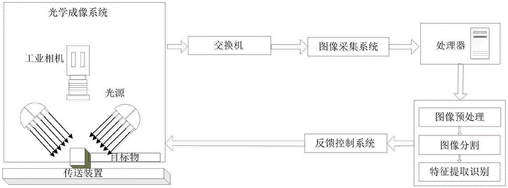
[0081] refer to figure 1 Shown, a kind of solar silicon wafer defect detection system comprises: visual image acquisition system, image processing system and sorting system; Described visual image acquisition system is used for automatically collecting the image of silicon wafer on silicon wafer automatic production line, described The image processing system is used to analyze the collected silicon wafer image, and automatically identify the silicon wafer image, and send the identified signal to the sorting system, and the sorting system is used to execute the signal of the image processing system to sort out the defective Silicon wafers with the same defects are sorted into the same sorting box to achieve precise sorting of silicon wafers.

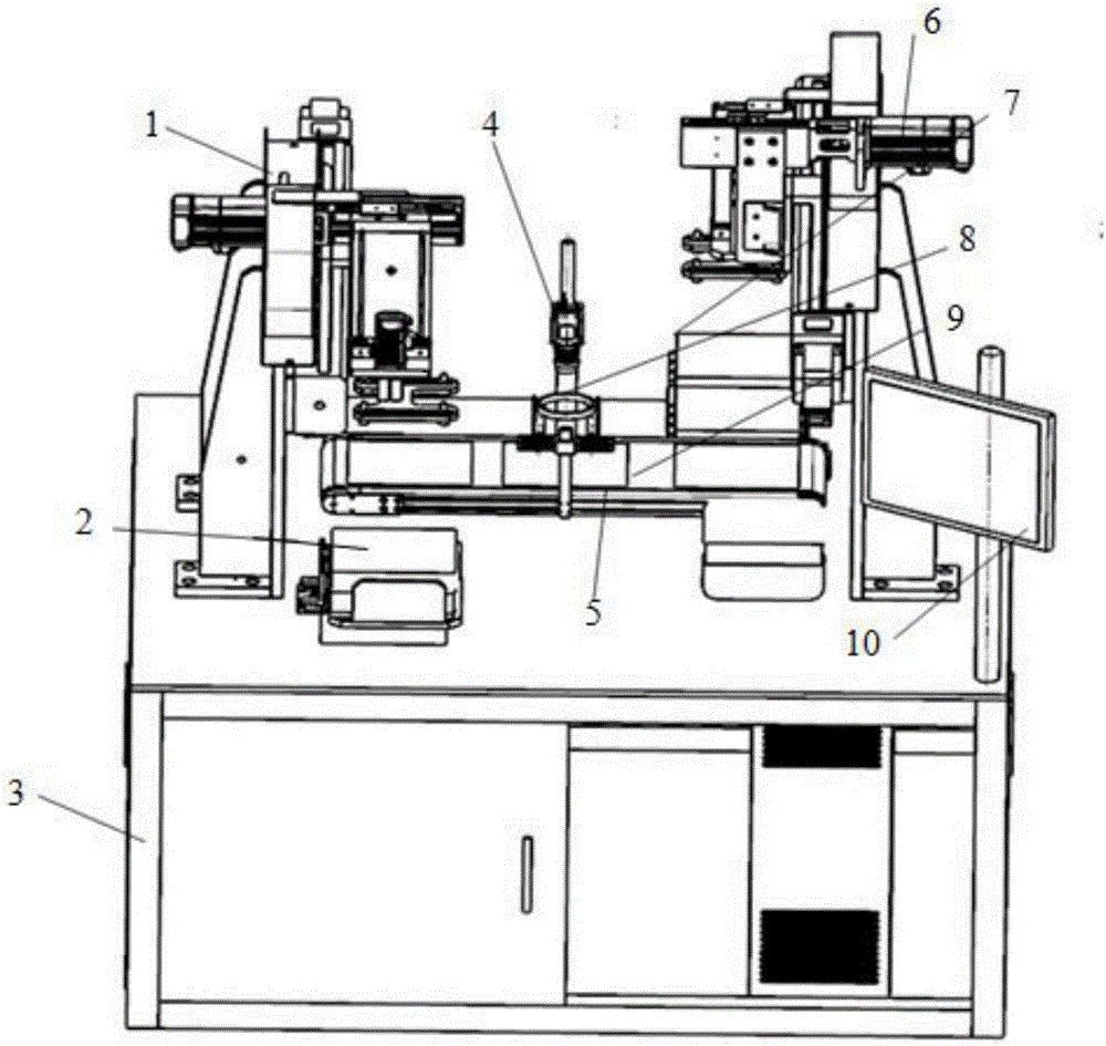
[0082] refer to figure 1 and figure 2 As shown, the visual image acquisition system includes a loading robot arm 1, a material tank 2, a material table 3, an indus...

Embodiment 2

[0084] Embodiment 2: A solar silicon wafer defect detection method.

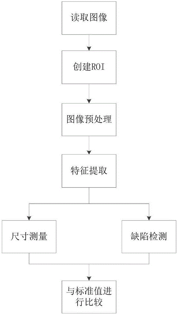
[0085] refer to image 3 As shown, a detection method carried out based on the solar silicon wafer defect detection system provided by the present invention specifically includes the following steps:

[0086] S1. The loading robot arm 1 grabs the silicon wafer 5 from the material tank 2 and puts it on the conveyor belt 9, and the motor controls the conveyor belt 9 to send the silicon wafer 5 to be detected to the detection station directly below the industrial camera 4;

[0087] S2. The PLC controls the industrial camera 4 to take pictures according to the in-place signal, and the lighting source 8 flickers to obtain the silicon wafer image;

[0088] S3. For the obtained silicon wafer image, the image processing software automatically measures the geometric feature value of the silicon wafer, and the silicon wafer geometric feature value includes the length and width of the silicon wafer; compare the geomet...


PUM


Abstract

The invention provides a solar silicon wafer defect detecting system. The solar silicon wafer defect detecting system comprises a visual image acquisition system, an image processing system and a sorting system; the visual image acquisition system is used for automatically acquiring images of silicon wafers on an automatic silicon wafer production line; the image processing system is used for analyzing the acquired silicon wafer images, automatically identifying the silicon wafer images and sending identification signals to the sorting system; and the sorting system is used for executing the signals of the image processing system, sorting out defective silicon wafers and sorting the silicon wafers with the same defects into same sorting boxes to realize accurate sorting of the silicon wafers. The invention also provides a detecting method based on the solar silicon wafer defect detecting system disclosed by the invention; the silicon wafers can be conveyed rapidly and rapid defect detection of the silicon wafer images can be carried out; and a high-speed and high-precision visual detection requirement of the production line can be met.

Description

technical field [0001] The invention belongs to the technical field of solar cell production, and in particular relates to a solar silicon wafer defect detection system and detection method. Background technique [0002] Solar photovoltaic power generation technology plays an important role in solving remote areas without electricity and saving energy. The key equipment of photovoltaic power generation equipment is solar panels, and the key component of solar panels is silicon wafers. The quality of silicon wafers has a great impact on power generation efficiency. Due to the influence of silicon wafers in the production process, there are often appearance defects such as unqualified dimensions and chipping, black spots, and cracks. [0003] The traditional manual detection of silicon wafers has low precision, strong subjectivity, poor repeatability, cannot provide consistent detection results, and has a high rate of missed detection and false detection; to use machine vision...

Claims


Application Information

Patent Timeline
IPC IPC(8): H01L21/66H01L21/67
CPCH01L21/67271H01L22/12H01L22/20
Inventor 彭博王华龙周艳红杨海东李力
Owner 广东佛智芯微电子技术研究有限公司
Why Eureka
Try Eureka