Quantum dot light-emitting diode device and preparation method thereof

A quantum dot light-emitting and diode technology, applied in the field of quantum dots, can solve the problems of low luminous efficiency and limited contact area of ​​quantum dot devices, and achieve the advantages of increasing light coupling and light output efficiency, reducing dissociation excitons, and increasing contact area. Effect

Inactive Publication Date: 2017-02-15
TCL CORPORATION
View PDF4 Cites 2 Cited by
  • Summary
  • Abstract
  • Description
  • Claims
  • Application Information

AI Technical Summary

Problems solved by technology

[0006] In view of the above-mentioned deficiencies in the prior art, the object of the present invention is to provide a quantum dot light-emitting diode device and its preparation method, aiming to solve the p

Method used


Image

  • Quantum dot light-emitting diode device and preparation method thereof
  • Quantum dot light-emitting diode device and preparation method thereof
  • Quantum dot light-emitting diode device and preparation method thereof

Examples


Embodiment 1

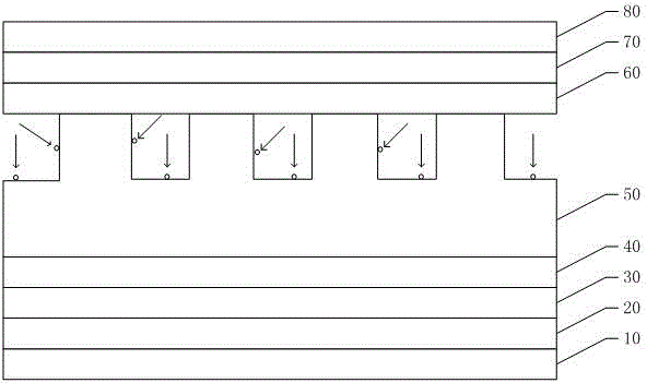
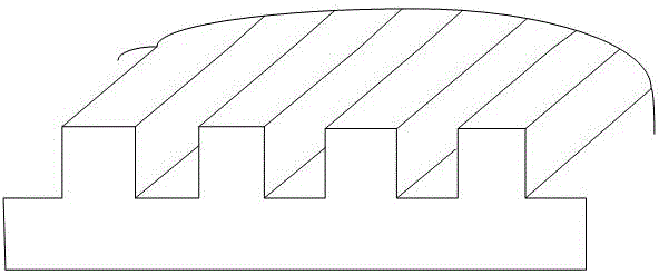
[0049] In a quantum dot light-emitting diode device, the glass substrate is 120nmITO; the thickness of the hole transport layer is 30nm, and one side of the quantum dot light-emitting layer is provided with periodically arranged elongated grooves, and the thickness of the quantum dot light-emitting layer is 20nm, the material of the quantum dot luminescent layer contains an intermediate core, the material is CdSe, and the outer shell material of the core is ZnS; the thickness of the electron transport layer is 30nm, and the electrode is Al.

Embodiment 2

[0051] In a quantum dot light-emitting diode device, the glass substrate is 120nmITO; the thickness of the hole transport layer is 30nm, and one side of the quantum dot light-emitting layer is provided with periodically arranged elongated grooves, and the thickness of the quantum dot light-emitting layer is 40nm, the material of the quantum dot light-emitting layer is an alloy body that may contain CdSe, CdS, ZnS, ZnSe; the thickness of the electron transport layer is 30nm, and the electrode is Al.

Embodiment 3

[0053] In a quantum dot light-emitting diode device, the glass substrate is 120nmITO; the thickness of the hole transport layer is 100nm, and one side of the quantum dot light-emitting layer is provided with periodically arranged elongated grooves, and the thickness of the quantum dot light-emitting layer is 60nm, the material of the quantum dot light-emitting layer is InP; the thickness of the electron transport layer is 100nm, and the electrode is Al.

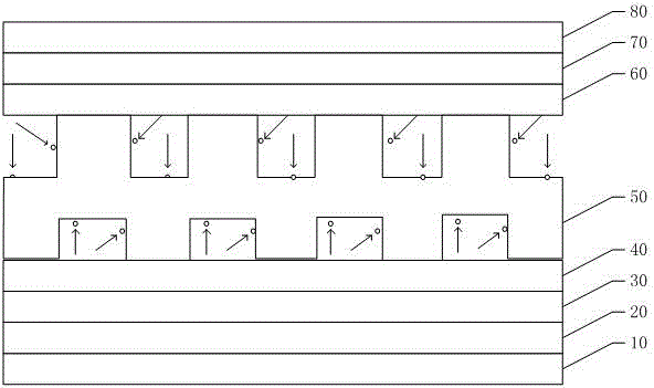
[0054] To sum up, the present invention provides a quantum dot light-emitting diode device and a preparation method thereof, by providing a plurality of grooves periodically arranged on at least one side of the quantum dot light-emitting layer, increasing the carrier transport layer and the quantum dot light-emitting layer The contact area between materials can improve the efficiency of carrier injection into the quantum dot light-emitting layer; it can also reduce the barrier of carrier transmission between quantum dots, so t...


PUM

PropertyMeasurementUnit
Thicknessaaaaaaaaaa
Thicknessaaaaaaaaaa
Thicknessaaaaaaaaaa

Abstract

The present invention discloses a quantum dot light-emitting diode device and a preparation method thereof. The device comprises a substrate, a bottom electrode, a hole injection layer, a hole transmission layer, a quantum dot luminescent layer, an electron transfer layer, an electron injection layer and a top electrode in order. The quantum dot luminescent layer at least has one surface provided with a plurality of periodically distributed grooves. Periodically distributed grooves are arranged in the luminescent layer to add the contact areas between the carrier transportation layer and the quantum dot luminescent layer materials so as to improve the efficiency of the carrier injection quantum dot luminescent layer; the transmission obstruction of the between the carriers between the quantum dots to allow more excitons to perform direct injection through the carriers or perform migration formation between short quantum dot; the quantum dot light-emitting diode device and the preparation method thereof can reduce the effect of exciton dissociation between the quantum dots; the quantum dot light-emitting diode device and the preparation method thereof can reduce the formation of lots of exciton-carrier three-body structure caused by carrier injection and imbalance transmission and reduce the exciton quenching; and moreover, the quantum dot light-emitting diode device and the preparation method thereof can employ the raster coupling principle to add the optical coupling of the diode and the emission efficiency.

Description

technical field [0001] The invention relates to the technical field of quantum dots, in particular to a quantum dot light-emitting diode device and a preparation method thereof. Background technique [0002] Quantum dot luminescent materials based on inorganic nanocrystals have the advantages of saturated color of emitted light, adjustable wavelength, and high photoluminescence and electroluminescence quantum yields, which are suitable for high-performance display devices; from the perspective of preparation technology, quantum dot luminescent materials are suitable for Spin coating, printing, and printing equipment under non-vacuum conditions; therefore, quantum dot light-emitting diodes (QLEDs) prepared with quantum dot films have become a strong competitor for next-generation display technologies. [0003] A QLED device generally includes an electrode 1 , a hole injection and hole transport layer, a light emitting layer, an electron transport and electron injection layer ...

Claims


Application Information

Patent Timeline
IPC IPC(8): H01L51/50H01L51/52H01L51/56
CPCH10K50/115H10K50/85H10K50/854H10K71/00
Inventor 陈崧钱磊杨一行曹蔚然向超宇
Owner TCL CORPORATION
Why Eureka
Try Eureka