
Wafer level packaging based MEMS wind speed and wind direction sensor structure and packaging method

A wafer-level packaging, wind speed and direction technology, used in instruments, measurement devices, and the use of thermal variables to measure fluid velocity, etc., can solve problems such as affecting sensor performance, affecting sensor sensitivity and response time, and reducing power consumption and cost. Effect

Inactive Publication Date: 2017-02-22
SOUTHEAST UNIV
View PDF7 Cites 14 Cited by
  • Summary
  • Abstract
  • Description
  • Claims
  • Application Information

AI Technical Summary

Problems solved by technology

In the past, the back of the silicon-sensitive chip was attached to the front of the ceramic, and the back of the ceramic was exposed to wind. In this way, the heat of heating needs to be transferred from the heating surface of the silicon to the other side and then to the ceramic, and then under the action of the wind field, the ceramic back generates The temperature difference will be transmitted back to the heating surface of the silicon for detection, which will affect the sensitivity and response time of the sensor, and since the silicon chip is attached to the ceramic chip with thermal conductive adhesive, the thermal conductive adhesive cannot be completely sealed during the packaging process. Symmetry, also affects sensor performance

Method used


Image

  • Wafer level packaging based MEMS wind speed and wind direction sensor structure and packaging method
  • Wafer level packaging based MEMS wind speed and wind direction sensor structure and packaging method
  • Wafer level packaging based MEMS wind speed and wind direction sensor structure and packaging method

Examples


Embodiment Construction

[0039] The present invention will be further described below in conjunction with the accompanying drawings and specific embodiments.

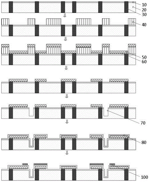
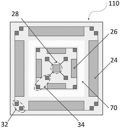
[0040] Such as Figure 1-6As shown, a MEMS wind speed and direction sensor structure based on wafer-level packaging, including a silicon chip 110 and a ceramic chip;

[0041] The silicon chip 110 includes a silicon wafer 20 and a silicon dioxide thermal insulation layer 10, the silicon dioxide thermal insulation layer 10 is arranged on the silicon wafer 20, and the silicon dioxide thermal insulation layer 10 is provided with a heating element 26 for generating heat. Temperature measuring element 28 and heat sensing temperature measuring element 24, a central temperature measuring element 28 is located at the center of the square silicon chip 110, four heating elements 26 and four heat sensing temperature measuring elements 24 are all centered on the central temperature measuring element 28 The center of the center is uniformly arranged at the ...


PUM


Abstract

The invention discloses a water level packaging based MEMS wind speed and wind direction sensor structure and packaging method. The method comprises the following steps. The front side of a silicon wafer is reversely welded in the wafer level packaging manner onto a ceramic substrate; the back side of the ceramic substrate is used as an interface where the sensors are in contact with the wind. Only through the low temperature bonding between the silicon wafer and the ceramic substrate and among the sensors in different areas, the silicon chip is capable of connecting the central temperature measuring device, the heating device and the heat transmitting and temperature measuring device to a circuit to perform control and detection. In order to achieve better heat contact between the silicon chip and the ceramic substrate, the heating ends of the heating device, the central temperature measuring device and the heat transmitting and temperature measuring device are closely attached to the ceramic substrate. In this way, compared with the structure in the prior art, cost can be reduced; sensitivity is increased; and the response time is shortened. The wafer level packaging based MEMS wind speed and wind direction sensor of the invention is cost-effective and highly sensitive. It also responds quickly and can be manufactured with simple technology.

Description

technical field [0001] The invention belongs to the technical field of sensors for measuring wind speed and direction, and in particular relates to a wafer-level packaging-based MEMS wind speed and direction sensor structure and packaging method. Background technique [0002] Wind speed and wind direction are very important parameters to reflect meteorological conditions, and have an important impact on environmental monitoring, transportation, and industrial and agricultural production. Therefore, it is of great practical significance to quickly measure wind speed and wind direction. However, since the unevenness of wind speed is very common, there will be large wind speed differences in the same area hundreds of meters apart. Therefore, large-scale sensing nodes are required to obtain more accurate wind speed and wind direction. The traditional mechanical wind cup was used in the early stage, and the wind speed detection system based on the principle of ultrasound and Dopp...

Claims


Application Information

Patent Timeline
IPC IPC(8): G01P5/12G01P13/02
CPCG01P5/12G01P13/02
Inventor 高适萱叶一舟黄庆安秦明
Owner SOUTHEAST UNIV
Learn More