

Light-emitting diode chip and manufacturing method thereof
A technology for light-emitting diodes and a manufacturing method, which is applied to electrical components, circuits, semiconductor devices, etc., can solve the problems affecting the photoelectric conversion efficiency of LED chips, low external quantum efficiency of LED chips, and inability to emit light from LED chips, etc. Efficiency, high refractive index contrast, effect of reducing dislocations and defects
- Summary
- Abstract
- Description
- Claims
- Application Information
AI Technical Summary
Problems solved by technology
Method used
Image

Examples
Embodiment 1
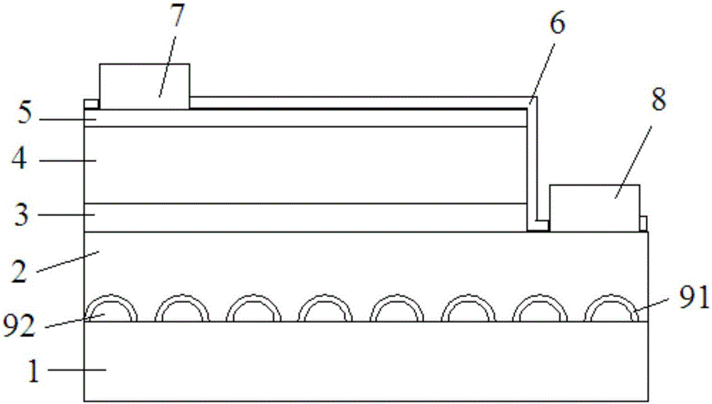
[0037] An embodiment of the present invention provides a light-emitting diode chip, which is suitable for display screens, backlight sources, white light lighting, etc., see figure 1 The light-emitting diode chip includes a substrate 1, and an n-type group III nitride semiconductor layer 2, an active layer 3, a p-type group III nitride semiconductor layer 4, a current spreading layer 5, and an insulating layer stacked on the substrate 1 in sequence. In the passivation layer 6, the p-type group III nitride semiconductor layer 4 is provided with a groove extending to the n-type group III nitride semiconductor layer 2, the first electrode 7 is arranged on the n-type group III nitride semiconductor layer 2, and the second The two electrodes 8 are disposed on the transparent conductive layer 5 .
[0038] In this embodiment, the light-emitting diode chip further includes a light extraction enhancement layer disposed between the substrate 1 and the n-type Group III nitride semiconduc...
Embodiment 2
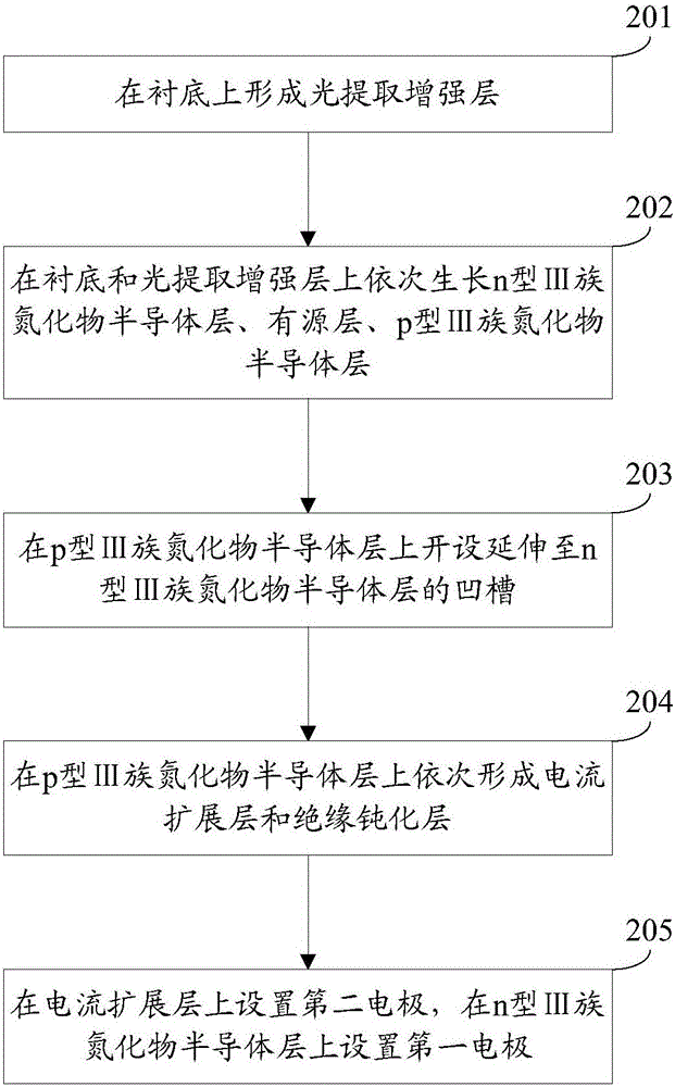
[0057] An embodiment of the present invention provides a method for manufacturing a light-emitting diode chip, which is suitable for manufacturing the light-emitting diode chip provided in Embodiment 1. Refer to figure 2 , the manufacturing method includes:
[0058] Step 201: forming a light extraction enhancement layer on a substrate.
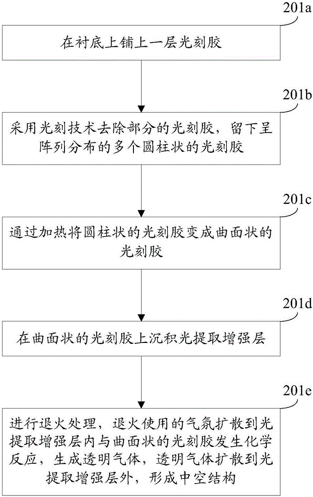
[0059] In this embodiment, the light extraction enhancement layer includes a plurality of curved surface structures distributed in an array, and the curved surface structures together with the substrate form a hollow structure, and the substrate, curved surface structures, and substances in the hollow structure are all transparent.
[0060] Alternatively, the substance within the hollow structure may be air.
[0061] Optionally, the material used for the curved surface structure can be Al 2 o 3 Or AlN.
[0062] Alternatively, the substrate can be Al 2 o 3 crystals.
[0063] Optionally, see image 3 , the step 201 may include:
[0064...
PUM
 Abstract
Description
Claims
Application Information