
Circuit substrate, and noise reduction method for circuit substrate

A technology for circuit substrates and core substrates, applied in printed circuits, circuit devices, multilayer circuit manufacturing, etc., can solve problems such as electromagnetic noise interference with analog circuits, signal degradation, etc., and achieve the smallest first electromagnetic band gap structure by utilizing installation space. the effect of

Active Publication Date: 2017-02-22
YAMAHA CORP
View PDF11 Cites 0 Cited by
  • Summary
  • Abstract
  • Description
  • Claims
  • Application Information

AI Technical Summary

Problems solved by technology

[0004] Accordingly, there is a problem that electromagnetic noise generated by an operating clock of a central processing unit (CPU), a memory, etc. in a digital circuit interferes with an analog circuit, thereby degrading a signal for communication

Method used


Image

  • Circuit substrate, and noise reduction method for circuit substrate
  • Circuit substrate, and noise reduction method for circuit substrate
  • Circuit substrate, and noise reduction method for circuit substrate

Examples


Embodiment Construction

[0032] Embodiments of the present invention will be described below with reference to the accompanying drawings.

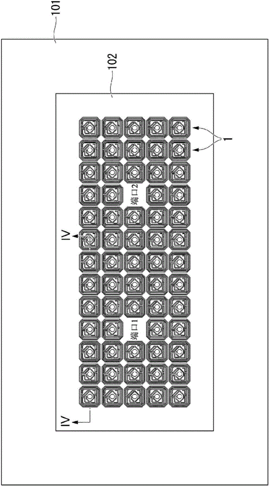
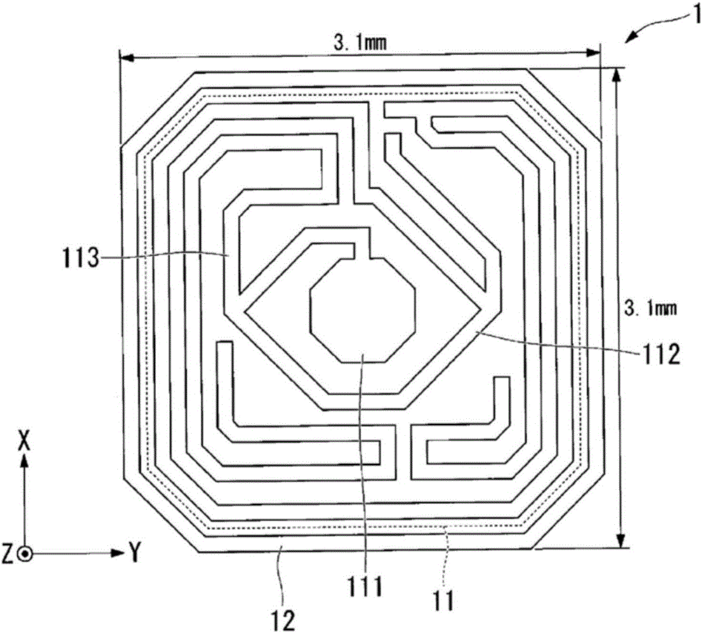
[0033] figure 1 is a plan view showing an example of a printed circuit board according to an embodiment of the present invention. figure 1 is according to the embodiment described below so that Figure 9 A more concrete diagram of the construction of , while Figure 9 It is a conceptual diagram of the basic configuration of the artificial magnetic conductor according to the present invention which will be described below. On an upper portion of one main surface (front surface) of a reference plane (for example, a ground plane) 101, a power supply plane 102 is provided in an overlapping manner. The power supply plane 102 is arranged such that one main surface (rear surface) thereof faces the upper surface (front surface) of the reference plane 101 . The power plane 102 is arranged such that the electromagnetic bandgap structures 1 are arranged in a matrix on th...


PUM


Abstract

Provided are: a circuit substrate with which an increase in the size of the area allocated to electromagnetic band gap structures formed from spiral open stubs can be inhibited, and mounting space can be utilized more effectively, even in cases when the frequency of the electromagnetic noise to be reduced is set so as to be further towards a low frequency side; and a noise reduction method for the circuit substrate. The circuit substrate of the invention of the present application is provided with: a core substrate; a reinforcing dielectric layer provided to one surface of the core substrate; first electromagnetic band gap structures which are provided to either of the surfaces of the reinforcing dielectric layer, and which suppress electromagnetic noise of a prescribed first frequency propagating in the core substrate; and auxiliary patterns which are formed around the outer peripheries of patterns forming the first electromagnetic band gap structures, with a prescribed distance therebetween.

Description

technical field [0001] The present invention relates to a circuit board on which electronic components are mounted and a noise reduction method for the circuit board. Background technique [0002] According to the demand for miniaturization of electronic components, a large number of integrated circuit chips or circuit components need to be mounted on an electronic circuit substrate on which semiconductor integrated circuits or circuit components are mounted. Therefore, there is an increasing demand for effective utilization of wiring space or installation space. [0003] In particular, in wireless local area network (LAN) communication, signals used for information processing by electronic circuits are digital signals, and therefore, analog circuits performing wireless communication and digital circuits performing information processing of signals used for communication are used simultaneously. [0004] Accordingly, there is a problem that electromagnetic noise generated b...

Claims


Application Information

Patent Timeline
Patent Type & Authority Applications(China)
IPC IPC(8): H05K3/46H05K1/02H05K1/16
CPCH05K1/0236H05K1/0298H05K1/16H05K1/025
Inventor 川田章弘
Owner YAMAHA CORP
Learn More