Tunable waveguide grating based on silicon waveguide-graphene

A technology of silicon waveguide and graphene, applied in optics, nonlinear optics, instruments, etc., can solve the problems of narrow tunable wavelength range of grating, inconvenient integration of grating structure, slow response speed, etc., and achieve wide tunable wavelength range, structural Compact, responsive effects

Inactive Publication Date: 2017-03-15
UNIV OF ELECTRONICS SCI & TECH OF CHINA
View PDF1 Cites 14 Cited by
  • Summary
  • Abstract
  • Description
  • Claims
  • Application Information

AI Technical Summary

Problems solved by technology

[0006] In order to solve the problems of narrow tunable wavelength range of the grating, slow response speed and inconvenient integration of the grating structure in the prior art, the present invention proposes a tunable waveguide grating based on silicon waveguide-graphene

Method used


Image

  • Tunable waveguide grating based on silicon waveguide-graphene
  • Tunable waveguide grating based on silicon waveguide-graphene
  • Tunable waveguide grating based on silicon waveguide-graphene

Examples


Embodiment 1

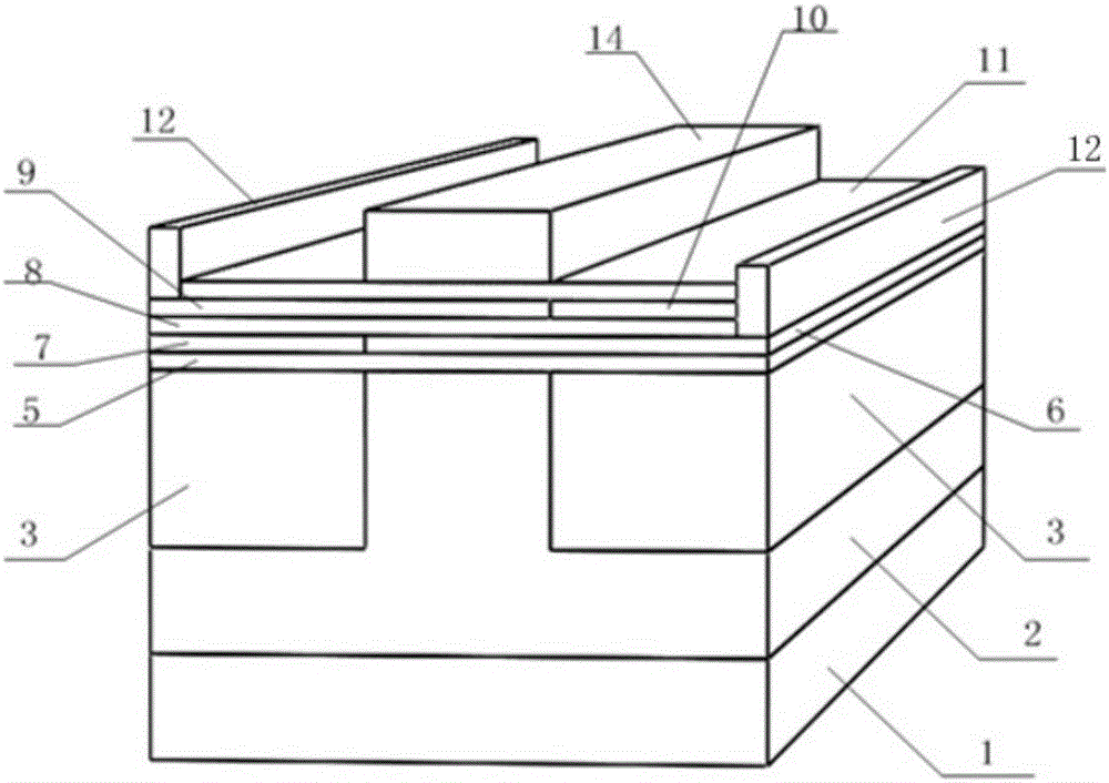
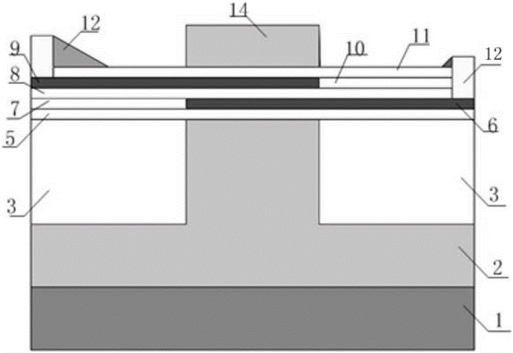
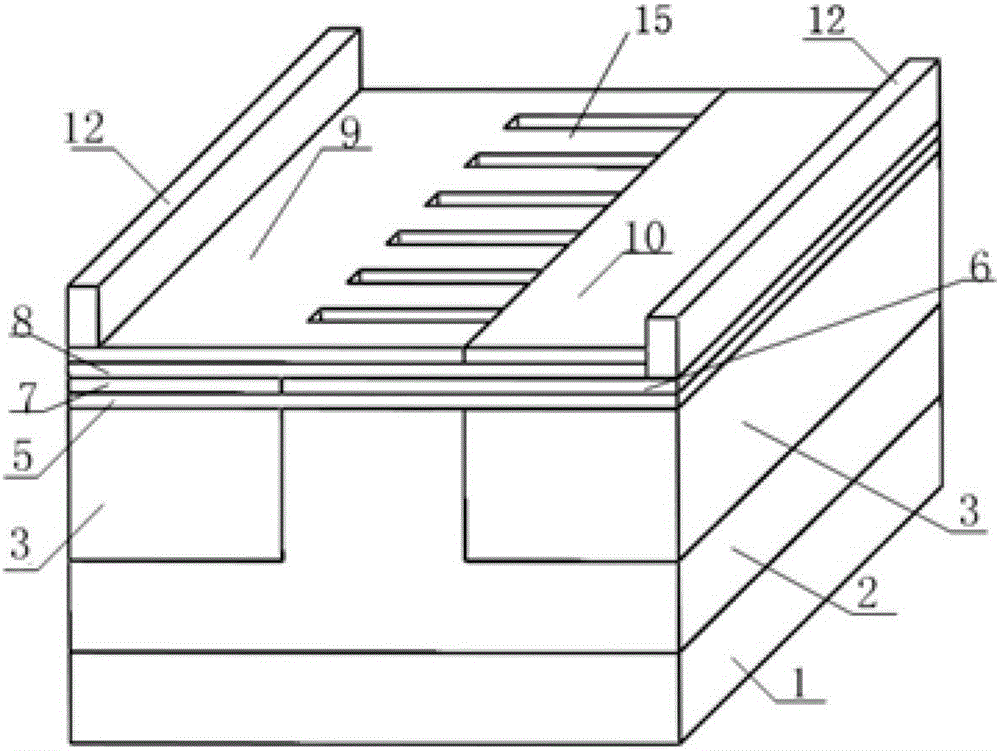
[0038] combined with figure 1 And attached figure 2, the material of the substrate 1 of the silicon-based waveguide grating in this embodiment is silicon dioxide, and the width of the ridge area of ​​the core layer ridge waveguide is set on the silicon dioxide substrate to be 0.6 μm, and the height of the ridge is 0.25 μm. Half of the waveguide 2 is laid with a 5nm thick first isolation dielectric layer 5, the material is hexagonal boron nitride (hBN), the first graphene layer 6 and the second graphene layer 9 are single-layer graphene, respectively Laid on the first isolation dielectric layer 5 and the third isolation dielectric layer 8, the second isolation dielectric layer, the third isolation dielectric layer, the fourth isolation dielectric layer, and the fifth isolation dielectric layer are all hexagonal nitrogen layers with a thickness of 5 nm. boron (hBN), the first graphene layer 6 and the second graphene layer 9 extend from both sides to connect the first electrode...


PUM

PropertyMeasurementUnit
thicknessaaaaaaaaaa

Abstract

The invention discloses a tunable waveguide grating based on silicon waveguide-graphene, and belongs to the technical field of optoelectronic devices. The tunable waveguide grating aims at relieving the problems that an existing grating is narrow in tunable wavelength range and low in response speed, and the grating structure is inconvenient to integrate. The waveguide grating of the same structure has different selectivities on light waves under different electric field conditions, and the reflecting wavelength of the grafting is changed. The tunable waveguide grating comprises a substrate, a ridge-shaped silicon waveguide is arranged on the substrate and comprises a ridge area lower half waveguide body and a ridge area upper half waveguide body, the ridge area lower half waveguide body is covered with a wrapping layer, the ridge area lower half waveguide body is sequentially provided with a first isolating dielectric layer, a first graphene layer, a third isolating dielectric layer, a second graphene layer and a fifth isolating dielectric layer from bottom to top, and a ridge area upper half rectangular waveguide body is arranged on the fifth isolating dielectric layer. The first graphene layer and the second graphene layer are both of an interdigital electrode structure, and interdigitals of the interdigital electrode structures are periodically arranged at equal intervals.

Description

technical field [0001] The invention belongs to the technical field of optoelectronic devices, in particular to a tunable waveguide grating based on silicon waveguide-graphene. Background technique [0002] Grating refers to a diffraction system with periodic changes in spatial structure or distribution of optical parameters (such as refractive index), which can reflect, refract, interfere and diffract light, and play an important role in the regulation of optical signals. In optical fiber communication, Gratings have important applications in semiconductor lasers, waveguide input and output couplers, beam splitters, polarization splitters, filters, optical add and drop filters, and sensing. [0003] The traditional grating is to form grooves on the surface of the grating by photolithography. After the grating is successfully fabricated, its structure and period remain unchanged. Since the resonant wavelength of the grating is only related to the period and effective refract...

Claims


Application Information

Patent Timeline
Patent Type & Authority Applications(China)
IPC IPC(8): G02F1/01G02F1/00
CPCG02F1/011G02F1/0018
Inventor 陆荣国刘天良田朝辉杨忠华叶胜威夏瑞杰张尚剑刘永
Owner UNIV OF ELECTRONICS SCI & TECH OF CHINA
Why Eureka
Try Eureka